Wideband receiver design requires a heterodyne architecture to obtain the best sensitivity in the presence of interference or blocking signals. Taking the design of a cellular cdma2000® multi-carrier receiver as an example, this article discusses some important parameters that affect the choice of analog-to-digital converter (ADC) —IF frequency, receiver analog power gain, signal bandwidth, and ADC sampling clock frequency. Through this design example, the following ADC parameters are also discussed: full-scale (FS) power, small signal noise floor (SSNF), signal-to-noise ratio (SNR), and spurious-free dynamic range (SFDR). The 16-bit, 80Msps MAX19586 ADC has the lowest noise floor of all ADCs today. There is no need to reduce gain or use automatic gain control (AGC) in receiver design. MAX19586's excellent noise performance and SFDR performance can meet the ADC requirements even for such applications.
The heterodyne receiver includes a first-level mixer (LO1) that converts the RF waveform to a first intermediate frequency (IF) signal (Figure 1). This IF signal can be digitized or sent to the second-stage mixer (LO2) to convert it to a lower frequency IF. Converting the signal to a lower IF takes advantage of the ADC's good noise and linear performance, which are generally only available at low frequency inputs. The undersampling technology is used to digitize the real bandpass signal, and its sampling rate conforms to Nyquist's law within the signal bandwidth, not its absolute frequency. Using this method, the ADC digitizes the real signal and then uses digital signal processing (DSP) technology to convert it into a composite component in the digital domain. The advantage of this method is that it can reduce the complexity and cost of the hardware, because the undersampling technology undertakes part of the down conversion task. However, this architecture requires an ADC with a higher clock rate and a wider dynamic range (that is, low noise and high linearity). In addition to these advantages, an important disadvantage of undersampling technology is noise aliasing. If the input signal is not sufficiently bandwidth limited, the aliasing noise in the band will be digitized and converted into a baseband signal together with the useful signal. Aliasing will cause the ADC's SNR to decrease.
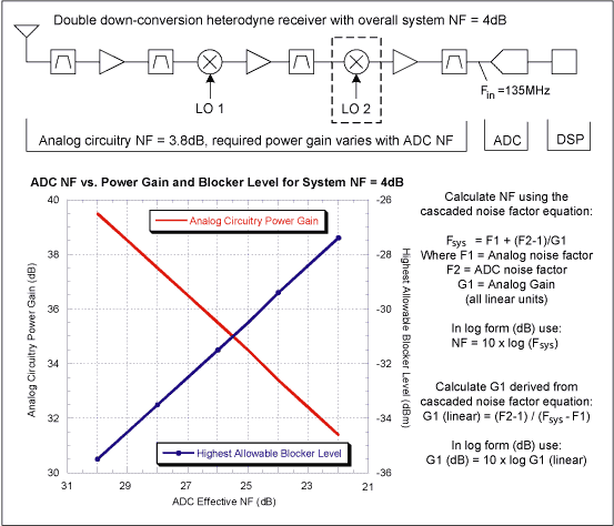
Figure 1. Using the characteristic curve to determine the optimal balance of ADC NF, receiver power gain, and maximum blocking level of a superheterodyne receiver.
The block diagram shown in Figure 1 is a typical secondary down-conversion receiver used in a cellular base station system. This type of receiver generally contains two identical receiving channels to provide diversity reception. If you cancel the second-stage mixer, you can get a frequency conversion architecture. Assume that the ADC needs to quantize three adjacent cdma2000 carriers, and the bandwidth of each carrier is about 1.23MHz. After conversion, these carrier signals will be filtered by a digital signal processor (DSP). For example, the clock rate of the ADC is 64 times the cdma2000 carrier code rate of 1.2288 Msps, or 78.64 Msps. For undersampling receivers, the clock rate determines the Nyquist bandwidth (fCLK / 2), which is an important parameter for calculating the ADC equivalent noise figure (NF).
Assuming that the design goal of the system noise figure (NF) is 4dB, the noise figure provided by the analog circuit section is 3.8dB. In the case of ignoring blocking interference, in order to meet the requirements of the system's receiving sensitivity, only allow the ADC to add a noise figure of 0.2dB to the system. It should be noted that the 4dB noise figure is far better than the requirements of the 3GPP2 cdma2000 standard, but it represents the design goal of many cellular base station manufacturers in order to leave enough margin compared with the minimum requirements. Figure 1 shows the relationship between the analog power gain and ADC NF and the tolerable in-band interference (blocking) at the antenna end without meeting the design goals of the system noise figure (no automatic gain control is used). The requirements for analog circuit power gain depend on the equivalent noise figure of the ADC, which is calculated from the known full-scale power level (in dBm), SSNF, and conversion rate.
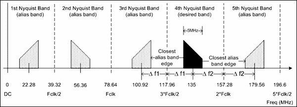
Figure 2. After the sampling frequency and intermediate frequency of the ADC are determined, various aliasing bands can be determined
Figure 2 shows the process of aliasing the unfiltered noise into the useful signal band, which will improve the SSNF of the ADC and reduce the signal-to-noise ratio (SNR). In the above example, the three cdma2000 RF carrier signals are down-converted to 135MHz and the bandwidth is 5MHz, and sent to the input of the ADC. The 2nd and 3rd harmonics of the input signal generated by the ADC will not alias into the useful signal band and can be ignored. Figure 2 shows only five Nyquist bands. In fact, signals up to 16 times the Nyquist frequency will be aliased into the useful signal bandwidth. Here, it is assumed that the ADC's full power input bandwidth reaches 600MHz. If these aliased signals are not properly attenuated, the noise performance of the ADC will be reduced.
Assume that the sampling frequency is 78.64Msps, the useful signal bandwidth is 5MHz, the aliasing frequency band is from DC to 629.12MHz (8 x fCLK), and the center frequencies are 22.28MHz, 56.36MHz, 100.92MHz, 179.56MHz ..., 606.84MHz. The center frequencies of the 3rd and 5th aliasing bands deviate from the Nyquist frequency edge, respectively  f1 and f2. In general, in addition to the useful signal at 135MHz, there are 15 other aliased signals. If only one aliased signal enters the input port of the ADC, it will increase the ADC noise figure NF by 10 x log (2), or 3dB. If all the noise in the band enters the ADC, the effective noise factor (NF) of the ADC will theoretically increase by 10 x log (15), or 11.8dB. At this time, it is assumed that the ADC quantizes the useful signal and each aliased noise signal the same.
In order to filter out the noise in the aliasing band, the attenuation near the high-side aliasing (> 177.06MHz) and low-side aliasing (<103.42MHz) bands should be no less than 16dB, so that the aliased signal has a greater impact on the ADC noise figure. The effect is less than 0.2dB. Higher attenuation can reduce the effect of aliased signal on ADC noise figure (NF) to a greater extent.
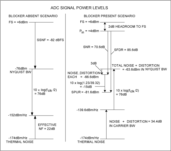
Figure 3. Sensitivity of ADC without blocking and sensitivity with strong blocking signal
Taking cdma2000 as an example, Figure 3 shows the requirements for ADC performance under the following two conditions: a) receiving sensitivity when there is no blocking; b) receiving sensitivity after the index decreases when there is blocking.
In order to calculate the equivalent noise figure of the ADC in the above two cases, it is assumed that the input matching resistance of the ADC is 200, and its full-scale (FS) power level is calculated. If the full-scale input voltage peak is 2.56VP-P, the corresponding full-scale input power is + 6dBm (RMS). When there is no blocking signal, the SSNF of the ADC is assumed to be -82dBFS. For a sampling frequency of 78.64Msps, the ADC noise floor level within the Nyquist bandwidth is -76dBm. Equivalent to a 1Hz bandwidth, the noise floor is -152dBm; compared with the thermal noise floor of -174dBm / Hz at room temperature, the equivalent noise figure of the ADC is 22dB, and it is assumed that all frequencies in the Nyquist band The noise spectrum remains flat. From this point of view, it is very difficult to achieve this noise figure index, but MAX19586 can fully meet the design requirements.
As can be seen from Figure 1, when the equivalent noise figure of the ADC is 22dB, in order to make the noise figure of the system reach 4dB, the analog circuit must provide a power gain of 31.4dB. Taking these factors into consideration, without using automatic gain control, the highest allowable effective blocking power of the system is -27.4dBm, as shown in the power level given in Figure 3:
FS-Margin-Gain = + 6dBm-2dB-31.4dB = -27.4dBm
In many receivers, if there is a higher level of blocking, you need to use an automatic gain control circuit to reduce the receiver's analog gain when there is a strong blocking signal. However, lowering the gain will result in an increase in the noise figure of the entire receiver, thereby reducing the desired receiver sensitivity. In multi-carrier receivers, under strong blocking signal conditions, reducing sensitivity is very detrimental to weak carrier signal extraction. If the ADC has a very low noise floor (such as MAX19586), the RF front-end gain requirement is lower under the same sensitivity conditions, so that the receiver can tolerate stronger blocking signals without using AGC.
When the in-band blocking signal and cdma2000 carrier appear at the antenna port at the same time, the 3GPP2 standard allows the reception sensitivity to be reduced by 3dB. The reduction of this index takes into account the increase in noise and distortion of analog circuits and ADC circuits. Assuming that 1dB is allocated to the analog circuit and 2dB to the ADC, the noise figure of the system (considering distortion) will be increased from 4dB to 7dB, and the gain is still 31.4dB; the noise figure of the analog circuit (considering distortion) is 4.8dB. From this, it can be calculated that when the system noise figure is 7dB, the noise figure (including distortion) of the ADC is 34.4dB, or -139.6dB / Hz (shown in Figure 3). In the Nyquist band, the equivalent noise (including distortion) level is -63.6dBm.
Assume that the noise and spurious power of the ADC has an effect on the overall ADC noise figure of 3dB, that is, the noise power in the Nyquist band is -66.6dBm. Comparing this power level with the 4dBm blocking signal at the ADC input port, we can get its signal-to-noise ratio requirement, 70.6dB. The calculation of the noise power in the useful signal band can be done as follows, dividing the cdma2000 signal bandwidth by the entire Nyquist bandwidth. In this case, the noise power in the carrier band is 10 x log (1.23MHz / 39.32MHz) or -15dB (-81.6dBm) lower than -66.6dBm. Because it is assumed that the noise and distortion power are equal, the spurious power is also -81.6dBm, so the SFDR index of the ADC is -85.6dB, as shown in Figure 3.
LED Street Lights offer longer operating lifetime, lower maintenance requirements and cost reductions over other bulbs. G-Lights has a wide variety of LED street lights for sale. LED street lights by G-Lights offer a long life span and extreme reliability, both important characteristics for street light selection. When you are interested in installing new LED Street Light, we offer a wide selection of LED street lights to choose from. LED street lighting comes in a variety of light distribution options, which is important in achieving the desired light cast. 5 year warranty provides you a good support for the project.
Led Street Light,Led Street Light Price List,Big Led Street Light,Led Street Light Price
ZHONGSHAN G-LIGHTS LIGHTING CO., LTD. , https://www.glightsled.com