Abstract: ApplicaTIons that require nonvolaTIle data storage almost always use an external serial EEPROM. This arTIcle describes how to provide nonvolaTIle data storage by using only the flash memory already available in the MAXQ microcontrollers.
IntroductionMost applications that require a microcontroller also require some mechanism to store settings that will be remembered even when power is removed. A radio, for example, that forgets its station presets when the battery is changed will not be successful in today's marketplace. Customers expect favorite stations, temperature presets, preferences, and other persistent information to be saved from one use to the next.
To meet this customer expectation for nonvolatile data storage, designers traditionally use a serial EEPROM. These EEPROM devices are small, inexpensive, and have a long history that makes the design engineer comfortable with their use. But in today's cost-sensitive marketplace, adding even an inexpensive EEPROM device to a design can break the budget.
Many processors use flash memory for storage of program code and static RAM for data storage. While it may be attractive to leverage unused parts of the flash memory for nonvolatile data storage, conventional Harvard architecture precludes this use. But the MAXQ architecture is a Harvard machine with separate code and data paths. MAXQ devices contain hardware that implements a pseudo-Von Neumann architecture, which allows easy access to code space as data memory. This extra versatility, combined with the MAXQ's utility functions that provide memory write and erase services, provides the background for a complete read-write, nonvolatile memory subsystem.
Basic Considerations About Flash MemoryFlash memory is a type of electrically erasable memory. It is generally considered to be "read-mostly." In simple terms, while flash memory is writable, its use assumes that data updates will be infrequent and that the bulk of operations will be read operations. Most flash memory devices are writable at the word level, but can only be erased an entire block at a time. This makes those memory devices generally unsuitable for variable storage, and suitable only for constant data tables that never change .
There are two kinds of flash memory: NAND flash and NOR flash. NAND flash is used in memory cards and flash drives. In general, reading from a NAND device requires several cycles as data is clocked out of the device serially. This sequential operation makes NAND flash unsuitable for the storage of program code, since the access time would be much too long. NOR flash, in contrast, resembles conventional byte- or word-wide memory. NOR flash can be read as one would read a ROM device: assert a device select and an address, and wait the access time before reading the data from the bus. NOR flash is used in the MAXQ processor family.
Flash Memory in MAXQ ProcessorsThe flash memory blocks used in the MAXQ processors erase to a "1" state. Consequently, after erasing, every location in the block will contain 0xFFFF. Programming a flash location changes some bits from a "1" to a " 0 "state. To return a programmed bit back to a" 1 "state, the entire block must be erased.
An issue that must be confronted with any electrically erasable memory device is endurance. Depending on the specific technology, a flash memory cell can endure as few as 1,000 or as many as 1,000,000 erase-program cycles before permanently failing. Any scheme that uses flash memory for data storage must therefore ensure that write cycles are evenly distributed about the array, and that no one set of locations is erased and programmed more often than another.
Most flash devices will permit any unprogrammed bit in a previously programmed location to be changed from a "1" to a "0" state. For example, most devices would allow a location programmed with the value 0xFFFE to be subsequently programmed with the value 0x7FFE , since that does not change any bit value from "0" to "1." The flash used in the MAXQ family devices, however, does not permit reprogramming a previously programmed location, even if no attempt is made to change a "0" bit back to a "1." Such a write attempt would fail, leaving the value at 0xFFFE.
There is a good reason for this programming restriction in MAXQ devices. The memory block being programmed is primarily used as code space, so it is prudent to forbid any write operation to a location that has been previously written. As the instruction 0xFFFF specifies an invalid source subdecode, it is unlikely to appear in a valid code block. Thus, blocking writes to a previously programmed location helps preserve the integrity of the code blocks.
Design Schemes Using the MAXQ2000In this article, we focus on one MAXQ device: the MAXQ2000. This microcontroller has 64kB of program storage organized as 128 blocks of 256 16-bit words. Two design schemes are presented below. The first scheme is suitable for information that is written once and then changed infrequently over the product lifetime, such as calibration data, version information, and feature strings. The second scheme is a more general mechanism designed to accommodate data that changes more frequently, such as usage information or detail records.
Scheme 1Problem: Calibration data needs to be stored in the product. From time to time, the product will require recalibration, so the calibration data must be stored in rewritable memory.
Solution: This is actually the simplest conceivable case. Two blocks in the MAXQ2000 program flash array are reserved for calibration data storage, one at word address 0x7E00 and the other at 0x7F00. The first time that a command is received to save the calibration data, the MAXQ2000 checks both blocks and discovers that they are both blank. The calibration data is saved to the first block.
At the second command to save calibration data, the MAXQ2000 once again checks both blocks. When it finds block 0 in use, it copies the calibration data to block 1 and then erases block 0.
When a request is received to read the calibration data (on power-up, for example), the MAXQ2000 reads both blocks to determine which is in use. Whichever block is not erased, is used to configure the device to its calibrated state.
The main advantage of this scheme is its simplicity. If the application requires a block configuration at power-up (or other configuration-restore events), this approach works well. The read routine accepts a word pointer and returns the value at that address; the write routine accepts a word pointer and attempts a write cycle at that address. The erase routine just erases both blocks.
There is a disadvantage to this scheme: the routines are extremely simple-minded. No attempt is made to determine if a write will succeed. The write is attempted, and if it fails, nothing is done to try to fix the problem. That limitation is why the scheme is only used for writes to a known blank block.
Scheme 2Problem: Nonvolatile storage is required to track energy usage and other frequently changing data. Updates occur from several times a week to several times a day. An electricity meter is a good example of the challenge.
Solution: This is a situation in which even conventional EEPROM would need help. The problem is this: the frequent updates and the fact that all electrically erasable memory technologies have limited write lifetimes preclude writing and erasing a single EEPROM cell over and over. Consider the case of an hourly update. An EEPROM with a 10,000 write-erase cycle limit would be exhausted in just over a year, well short of the ten-year design goal established for the electricity meter.
A solution to this problem is to implement some form of "wear leveling." This approach means that no single location is written over and over. Instead, write cycles are spread over the entire memory array with appropriate indexing similarly distributed.
Wear leveling is a well-understood technology and is used in flash storage devices just for this purpose. The algorithms can be complex and difficult to understand. But for our purposes, a much simpler mechanism will suffice.
Instead of being referenced by address, in this implementation data items in the storage array are referenced by data element number. A data element number is an arbitrary 8-bit value that uniquely identifies the data element. Thus in this scheme there can be a maximum of 255 data elements (data element 0 is reserved.) Each data element has: a two-byte header (see Figure 1) that contains the data element number and the data element length; a 2-bit code that indicates one, two, three, or four 16-bit words, with sufficient space remaining for error management if desired.
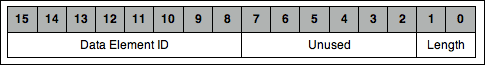
Figure 1. Structure of a Data Element header.
To write a data element, the write subroutine must know the data to be written, the length of the data element, and the location at which the data is to be written. It is simple to determine the address to which the data will be written ; data elements, whether a new element or an update to an existing element, are written to the end of the storage array. The write function seeks the end of the array, and then writes the new data element immediately following the last record. If there is insufficient space in the flash page to contain a record of the specified length, an end-of -page marker is written and a new page is opened. See Figure 2 for the structure of a typical data page.
In this data page, data element 1 was written first and is frequently updated. Data element 4 was written next, and has never been updated. Data element 3 was then written, and has been updated seven times. Finally, data element 2 has been written and never updated.
The presence of a page end marker indicates that a data write attempt was made, but that the data element was too long to fit on the page. A new page would have been opened to accommodate the data element. The end of the entire data structure is designated by a blank element where an element header is expected to be.
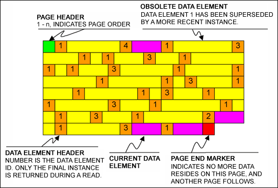
Figure. 2. A typical data page.
Note that this scheme has not addressed the issue of duplicate records. That is because duplicate records are not an issue. In fact, duplicate records are completely ignored by both the read and write routines. When writing, the new record goes at the end of the array, whether or not a same-numbered record already exists. When reading, only the last (and thus, most recent) record that matches the requested record number is retrieved.
Reading a data element from the array is somewhat more involved than writing. The read function accepts an element number and an address to which the contents of the data element should be written. When called, the read function searches the array from the beginning. When it finds a record that matches the requested data element, it stores the address and keeps searching. If it finds another matching record, the read function replaces the stored address with the new address. When the end of the array is reached, the stored address will point to the most recently written copy of the requested record. The read function then copies this data to the buffer passed when the function was called.
Although a workable read-mostly mechanism to store and retrieve records from a storage array has been presented, there remains one problem: there is no mechanism for reusing space occupied by obsolete copies of the records. (There is also no mechanism to delete a record , but as this scheme is structured to work in an embedded application, that is probably not a critical feature.) Without recovering some space, the allocated space will quickly be exhausted. Yet recovering space means erasing entire pages, since flash memory can only be erased one full page at a time. The problem is further complicated because flash pages cannot be arbitrarily erased without the risk of deleting useful information. The only option is to copy active information to a new page before erasing old pages.
Recovering space from obsolete records is a three-stage process. First, new flash pages are opened and the most recent versions of each data element are copied into the new pages. Second, the old pages are erased. Finally, page markers are placed on the new pages so that the read routine can find them.
The first stage is somewhat complex, and requires examination in more detail. A simple way to perform this step would be to divide it into two substeps: first, use a RAM array to store the record number and the address of the most recent record in the array; and second, step through the RAM array to copy the most recent records to the new flash pages. This process would be fast and relatively straightforward.
The problem with this two-substep scheme is that the MAXQ2000 has 1k word of RAM. The above scheme limits the amount of unique data that can be stored to the size of the RAM that can be spared for the buffer. This is clearly unacceptable.
The solution to this dilemma is time-consuming, but works regardless of how large (within reason) the storage array becomes. Instead of building a pointer list in RAM, make multiple passes through the source array for every unique entry. Thus, the compacting algorithm becomes: Read an element from the source array. Search for the element in the destination array. If found, that element has already been written. Increment the source pointer and go back to 1. Scan the source array for the latest copy of the element. Write the latest copy of the data element to the destination array. Increment the source pointer and go back to 1. At the end, there will be exactly one entry for each unique data element in the destination array. An illustration of a packed page is given in Figure 3. The source pages can now be safely erased and page headers written to the destination array.

Figure 3. Following space recovery, the data page of Figure 2 would appear like this.
This process has been structured to be as safe for the stored data as possible. There is, however, a danger that must be confronted when working with flash devices: power failure during a write or erase operation. If power fails, it is likely that one or more pages will be corrupted (in the case of a write) or incompletely erased (in the case of an erase operation). But the compact operation is inherently safe. Consider the following scenarios: If a power failure occurs during the packing operation , the source pages remain completely intact. After power restoration, the newly written pages can be easily identified (they have no page headers) and erased, and the pack operation restarted. If a power failure occurs while the old pages are being erased, they will probably contain invalid headers. These pages can be erased and headers added to the new pages. If a power failure occurs when page headers are being written to the new pages, the data remains intact. The page header update operat ion can be restarted. In short, there should be no mechanism through which unexpected events can irrecoverably corrupt array data.
Scheme 2 EnhancementsThe storage subsystem presented here has no error detection mechanism. There are bits available (six, as presented) in the data element identifier that are uncommitted. One could use a CRC6 algorithm (x6 + x + 1) to compute a CRC across the data element to ensure that no read or write errors have occurred. While this is not a particularly robust algorithm (it will miss one out of 64 multibit errors), it will detect most real-world errors likely to occur.
Another limitation to the system as given is that read access time is necessarily long. For every read, every record in the array must be read to find the most recent record. There are three methods to improve access time: Leave a blank word in the data element for a forward pointer. When the value is updated, fill in the forward pointer to the new entry. In this way, the table can be traversed as a linked list. Traverse the table backward. Now simply stop at the first occurrence of the requested element. If there is only a small number of unique elements, create a RAM array at startup that contains element IDs and pointers. Subsequent accesses are very fast. Just read the RAM array to determine where to obtain the data element. ConclusionNonvolatile data storage is a factor that every design engineer must confront sooner or later. With the MAXQ processor's flexible flash memory, there is no reason ever again to resort to small serial memories for storing configuration data.
A version of this application note was published on the Embedded.com website in January of 2008.
IntroductionMost applications that require a microcontroller also require some mechanism to store settings that will be remembered even when power is removed. A radio, for example, that forgets its station presets when the battery is changed will not be successful in today's marketplace. Customers expect favorite stations, temperature presets, preferences, and other persistent information to be saved from one use to the next.
To meet this customer expectation for nonvolatile data storage, designers traditionally use a serial EEPROM. These EEPROM devices are small, inexpensive, and have a long history that makes the design engineer comfortable with their use. But in today's cost-sensitive marketplace, adding even an inexpensive EEPROM device to a design can break the budget.
Many processors use flash memory for storage of program code and static RAM for data storage. While it may be attractive to leverage unused parts of the flash memory for nonvolatile data storage, conventional Harvard architecture precludes this use. But the MAXQ architecture is a Harvard machine with separate code and data paths. MAXQ devices contain hardware that implements a pseudo-Von Neumann architecture, which allows easy access to code space as data memory. This extra versatility, combined with the MAXQ's utility functions that provide memory write and erase services, provides the background for a complete read-write, nonvolatile memory subsystem.
Basic Considerations About Flash MemoryFlash memory is a type of electrically erasable memory. It is generally considered to be "read-mostly." In simple terms, while flash memory is writable, its use assumes that data updates will be infrequent and that the bulk of operations will be read operations. Most flash memory devices are writable at the word level, but can only be erased an entire block at a time. This makes those memory devices generally unsuitable for variable storage, and suitable only for constant data tables that never change .
There are two kinds of flash memory: NAND flash and NOR flash. NAND flash is used in memory cards and flash drives. In general, reading from a NAND device requires several cycles as data is clocked out of the device serially. This sequential operation makes NAND flash unsuitable for the storage of program code, since the access time would be much too long. NOR flash, in contrast, resembles conventional byte- or word-wide memory. NOR flash can be read as one would read a ROM device: assert a device select and an address, and wait the access time before reading the data from the bus. NOR flash is used in the MAXQ processor family.
Flash Memory in MAXQ ProcessorsThe flash memory blocks used in the MAXQ processors erase to a "1" state. Consequently, after erasing, every location in the block will contain 0xFFFF. Programming a flash location changes some bits from a "1" to a " 0 "state. To return a programmed bit back to a" 1 "state, the entire block must be erased.
An issue that must be confronted with any electrically erasable memory device is endurance. Depending on the specific technology, a flash memory cell can endure as few as 1,000 or as many as 1,000,000 erase-program cycles before permanently failing. Any scheme that uses flash memory for data storage must therefore ensure that write cycles are evenly distributed about the array, and that no one set of locations is erased and programmed more often than another.
Most flash devices will permit any unprogrammed bit in a previously programmed location to be changed from a "1" to a "0" state. For example, most devices would allow a location programmed with the value 0xFFFE to be subsequently programmed with the value 0x7FFE , since that does not change any bit value from "0" to "1." The flash used in the MAXQ family devices, however, does not permit reprogramming a previously programmed location, even if no attempt is made to change a "0" bit back to a "1." Such a write attempt would fail, leaving the value at 0xFFFE.
There is a good reason for this programming restriction in MAXQ devices. The memory block being programmed is primarily used as code space, so it is prudent to forbid any write operation to a location that has been previously written. As the instruction 0xFFFF specifies an invalid source subdecode, it is unlikely to appear in a valid code block. Thus, blocking writes to a previously programmed location helps preserve the integrity of the code blocks.
Design Schemes Using the MAXQ2000In this article, we focus on one MAXQ device: the MAXQ2000. This microcontroller has 64kB of program storage organized as 128 blocks of 256 16-bit words. Two design schemes are presented below. The first scheme is suitable for information that is written once and then changed infrequently over the product lifetime, such as calibration data, version information, and feature strings. The second scheme is a more general mechanism designed to accommodate data that changes more frequently, such as usage information or detail records.
Scheme 1Problem: Calibration data needs to be stored in the product. From time to time, the product will require recalibration, so the calibration data must be stored in rewritable memory.
Solution: This is actually the simplest conceivable case. Two blocks in the MAXQ2000 program flash array are reserved for calibration data storage, one at word address 0x7E00 and the other at 0x7F00. The first time that a command is received to save the calibration data, the MAXQ2000 checks both blocks and discovers that they are both blank. The calibration data is saved to the first block.
At the second command to save calibration data, the MAXQ2000 once again checks both blocks. When it finds block 0 in use, it copies the calibration data to block 1 and then erases block 0.
When a request is received to read the calibration data (on power-up, for example), the MAXQ2000 reads both blocks to determine which is in use. Whichever block is not erased, is used to configure the device to its calibrated state.
The main advantage of this scheme is its simplicity. If the application requires a block configuration at power-up (or other configuration-restore events), this approach works well. The read routine accepts a word pointer and returns the value at that address; the write routine accepts a word pointer and attempts a write cycle at that address. The erase routine just erases both blocks.
There is a disadvantage to this scheme: the routines are extremely simple-minded. No attempt is made to determine if a write will succeed. The write is attempted, and if it fails, nothing is done to try to fix the problem. That limitation is why the scheme is only used for writes to a known blank block.
Scheme 2Problem: Nonvolatile storage is required to track energy usage and other frequently changing data. Updates occur from several times a week to several times a day. An electricity meter is a good example of the challenge.
Solution: This is a situation in which even conventional EEPROM would need help. The problem is this: the frequent updates and the fact that all electrically erasable memory technologies have limited write lifetimes preclude writing and erasing a single EEPROM cell over and over. Consider the case of an hourly update. An EEPROM with a 10,000 write-erase cycle limit would be exhausted in just over a year, well short of the ten-year design goal established for the electricity meter.
A solution to this problem is to implement some form of "wear leveling." This approach means that no single location is written over and over. Instead, write cycles are spread over the entire memory array with appropriate indexing similarly distributed.
Wear leveling is a well-understood technology and is used in flash storage devices just for this purpose. The algorithms can be complex and difficult to understand. But for our purposes, a much simpler mechanism will suffice.
Instead of being referenced by address, in this implementation data items in the storage array are referenced by data element number. A data element number is an arbitrary 8-bit value that uniquely identifies the data element. Thus in this scheme there can be a maximum of 255 data elements (data element 0 is reserved.) Each data element has: a two-byte header (see Figure 1) that contains the data element number and the data element length; a 2-bit code that indicates one, two, three, or four 16-bit words, with sufficient space remaining for error management if desired.
Figure 1. Structure of a Data Element header.
To write a data element, the write subroutine must know the data to be written, the length of the data element, and the location at which the data is to be written. It is simple to determine the address to which the data will be written ; data elements, whether a new element or an update to an existing element, are written to the end of the storage array. The write function seeks the end of the array, and then writes the new data element immediately following the last record. If there is insufficient space in the flash page to contain a record of the specified length, an end-of -page marker is written and a new page is opened. See Figure 2 for the structure of a typical data page.
In this data page, data element 1 was written first and is frequently updated. Data element 4 was written next, and has never been updated. Data element 3 was then written, and has been updated seven times. Finally, data element 2 has been written and never updated.
The presence of a page end marker indicates that a data write attempt was made, but that the data element was too long to fit on the page. A new page would have been opened to accommodate the data element. The end of the entire data structure is designated by a blank element where an element header is expected to be.
Figure. 2. A typical data page.
Note that this scheme has not addressed the issue of duplicate records. That is because duplicate records are not an issue. In fact, duplicate records are completely ignored by both the read and write routines. When writing, the new record goes at the end of the array, whether or not a same-numbered record already exists. When reading, only the last (and thus, most recent) record that matches the requested record number is retrieved.
Reading a data element from the array is somewhat more involved than writing. The read function accepts an element number and an address to which the contents of the data element should be written. When called, the read function searches the array from the beginning. When it finds a record that matches the requested data element, it stores the address and keeps searching. If it finds another matching record, the read function replaces the stored address with the new address. When the end of the array is reached, the stored address will point to the most recently written copy of the requested record. The read function then copies this data to the buffer passed when the function was called.
Although a workable read-mostly mechanism to store and retrieve records from a storage array has been presented, there remains one problem: there is no mechanism for reusing space occupied by obsolete copies of the records. (There is also no mechanism to delete a record , but as this scheme is structured to work in an embedded application, that is probably not a critical feature.) Without recovering some space, the allocated space will quickly be exhausted. Yet recovering space means erasing entire pages, since flash memory can only be erased one full page at a time. The problem is further complicated because flash pages cannot be arbitrarily erased without the risk of deleting useful information. The only option is to copy active information to a new page before erasing old pages.
Recovering space from obsolete records is a three-stage process. First, new flash pages are opened and the most recent versions of each data element are copied into the new pages. Second, the old pages are erased. Finally, page markers are placed on the new pages so that the read routine can find them.
The first stage is somewhat complex, and requires examination in more detail. A simple way to perform this step would be to divide it into two substeps: first, use a RAM array to store the record number and the address of the most recent record in the array; and second, step through the RAM array to copy the most recent records to the new flash pages. This process would be fast and relatively straightforward.
The problem with this two-substep scheme is that the MAXQ2000 has 1k word of RAM. The above scheme limits the amount of unique data that can be stored to the size of the RAM that can be spared for the buffer. This is clearly unacceptable.
The solution to this dilemma is time-consuming, but works regardless of how large (within reason) the storage array becomes. Instead of building a pointer list in RAM, make multiple passes through the source array for every unique entry. Thus, the compacting algorithm becomes: Read an element from the source array. Search for the element in the destination array. If found, that element has already been written. Increment the source pointer and go back to 1. Scan the source array for the latest copy of the element. Write the latest copy of the data element to the destination array. Increment the source pointer and go back to 1. At the end, there will be exactly one entry for each unique data element in the destination array. An illustration of a packed page is given in Figure 3. The source pages can now be safely erased and page headers written to the destination array.
Figure 3. Following space recovery, the data page of Figure 2 would appear like this.
This process has been structured to be as safe for the stored data as possible. There is, however, a danger that must be confronted when working with flash devices: power failure during a write or erase operation. If power fails, it is likely that one or more pages will be corrupted (in the case of a write) or incompletely erased (in the case of an erase operation). But the compact operation is inherently safe. Consider the following scenarios: If a power failure occurs during the packing operation , the source pages remain completely intact. After power restoration, the newly written pages can be easily identified (they have no page headers) and erased, and the pack operation restarted. If a power failure occurs while the old pages are being erased, they will probably contain invalid headers. These pages can be erased and headers added to the new pages. If a power failure occurs when page headers are being written to the new pages, the data remains intact. The page header update operat ion can be restarted. In short, there should be no mechanism through which unexpected events can irrecoverably corrupt array data.
Scheme 2 EnhancementsThe storage subsystem presented here has no error detection mechanism. There are bits available (six, as presented) in the data element identifier that are uncommitted. One could use a CRC6 algorithm (x6 + x + 1) to compute a CRC across the data element to ensure that no read or write errors have occurred. While this is not a particularly robust algorithm (it will miss one out of 64 multibit errors), it will detect most real-world errors likely to occur.
Another limitation to the system as given is that read access time is necessarily long. For every read, every record in the array must be read to find the most recent record. There are three methods to improve access time: Leave a blank word in the data element for a forward pointer. When the value is updated, fill in the forward pointer to the new entry. In this way, the table can be traversed as a linked list. Traverse the table backward. Now simply stop at the first occurrence of the requested element. If there is only a small number of unique elements, create a RAM array at startup that contains element IDs and pointers. Subsequent accesses are very fast. Just read the RAM array to determine where to obtain the data element. ConclusionNonvolatile data storage is a factor that every design engineer must confront sooner or later. With the MAXQ processor's flexible flash memory, there is no reason ever again to resort to small serial memories for storing configuration data.
A version of this application note was published on the Embedded.com website in January of 2008.
MAXQ is a registered trademark of Maxim Integrated Products, Inc.
12V Power Adapter,Catv Linear Power Adapter,Linear Mode Power Adapter,Catv Linear Mode Power Adapter
Ninghai Yingjiao Electrical Co., Ltd. , https://www.yingjiaoadapter.com