Abstract: This article discusses a typical power supply architecture in automotive applications, and discusses how to add an active voltage limiting function to the basic power supply design, and clarifies the need for an integrated voltage limiter. Several examples of Maxim's active voltage limiter design are also provided.
Overview-Typical Automotive Power Supply Architecture Figure 1 shows a simplified block diagram of a typical automotive power supply.
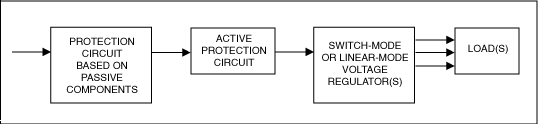
Figure 1. Basic schematic diagram of automotive power supply
The above block diagram mainly includes the following units: Passive protection circuit: limit the positive voltage of the + 12V power bus and prevent the generation of negative voltage. Active protection circuit: The function of the voltage limiter is similar to the passive protection circuit, but it uses active devices such as transistors, which can provide a better price-performance ratio and a smaller size than a passive solution with the same function. Switching mode or linear regulator: provide the appropriate voltage and current for the specified load, may use a multi-channel power supply structure. In different applications, the technical specifications of these components will be different. Some applications do not consider these factors, but they will have a negative impact on the overall electrical performance of the system. In fact, any missing of the above unit circuit will increase the complexity of the system design.
The principle of integrating a voltage limiter active voltage limiter in the power supply is very simple. A MOSFET is added between the input and output of the device, and the limiter controls the gate of the field effect tube. Under normal working conditions, turn on the MOSFET and supply power to the load; if the voltage exceeds the defined threshold, the voltage limiting circuit will turn off the external MOSFET and disconnect the power supply from the load.
Figure 2 shows the internal structure and typical application circuit of the basic voltage limiting circuit.
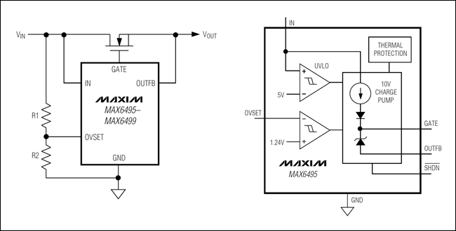
Figure 2. 72V application example. An external MOSFET is used as an overvoltage protection switch / limiter control. The MAX6495–MAX6499 circuit diagram provides the device's overvoltage detection method. The MAX6495 circuit diagram shows the internal structure of the device.
In this basic voltage limiting circuit, VIN supplies power to the internal circuit, and the maximum voltage of VIN is 80V. The voltage divider at the OVSET terminal sets the overvoltage detection threshold, and the built-in charge pump supplies power to the gate drive of the low-cost n-channel MOSFET, thereby reducing system cost. In addition to providing overvoltage thresholds, these ICs also provide undervoltage detection thresholds.
In another solution, a window-type voltage limiter with adjustable threshold is used. Figure 3 shows a related application example.
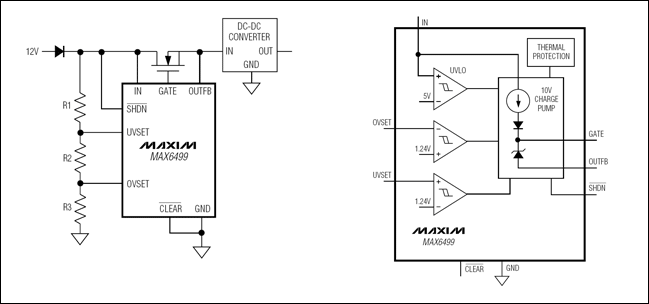
Figure 3. The MAX6499 is configured as an overvoltage / undervoltage window detector (left), and its basic functional block diagram is shown on the right.
In this case, the voltage-limiting circuit can prevent the MOSFET and the load from operating in undervoltage and overvoltage conditions. The output voltage range can be strictly limited (limited to a narrower range) to reduce the technical requirements for the input range of the voltage regulator, thereby reducing the design cost of the voltage regulator. In some audio applications, high-precision voltage regulation is not required. For these applications, the design of the voltage limiting circuit can eliminate the voltage regulator circuit.
As mentioned above, the voltage divider can control the input voltage of the IC shown in FIG. 2, and the voltage divider can also be connected to the output of the voltage limiter, as shown in FIG. In the latter example, the voltage divider limits the voltage on the load instead of simply turning it off. It can be seen from the performance test data that the voltage limit detection is performed periodically. The oscillation period is determined by the load capacitance and load current and can be varied within a wide range. The periodic oscillation includes two stages; the first stage puts the MOSFET into an effective mode, and the second stage turns it off.
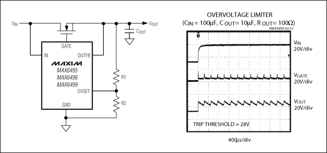
Figure 4. The device is configured as an overvoltage limiting protection switch with CIN = 100µF, COUT = 10µF, and ROUT = 100Ω.
The circuit configuration shown in Figure 4 causes the MOSFET to periodically enter an effective mode to dissipate power on the MOSFET. The heat dissipation of the MOSFET needs to be considered. For this reason, the IC contains a high-temperature protection unit with a threshold of approximately + 160 ° C. When the temperature drops below + 140 ° C, the circuit returns to normal mode. In order to optimize the design, the IC should be placed close to the MOSFET so that both have a good thermal conduction path.
As we all know, the circuit board power bus may have negative voltage spikes or positive voltage spikes. Passive devices or special ICs can be used for protection circuits that suppress negative voltages. Figure 5 provides the internal structure of the MAX6496 reverse voltage protection.
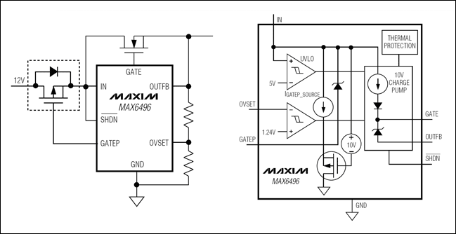
Figure 5. Using the MAX6496 to achieve overvoltage limiting, with voltage drop reverse protection (left); the right is a functional block diagram.
In addition to limiting the forward voltage, the MAX6496 also includes a p-channel MOSFET gate control circuit that keeps the MOSFET on when it is positive and off when it is negative. At high load currents and low input voltages, this circuit is more practical than typical Schottky diodes.
Conclusion The voltage limiting circuits discussed in this article provide corresponding characteristic parameters, which are convenient for the application of the device in various occasions. Each voltage limiting circuit allows a maximum input voltage of 72V when the load is powered on, and a maximum input voltage of 80V when the load is cut off. The following table summarizes the main characteristics of voltage limiting ICs.
Overview-Typical Automotive Power Supply Architecture Figure 1 shows a simplified block diagram of a typical automotive power supply.
Figure 1. Basic schematic diagram of automotive power supply
The above block diagram mainly includes the following units: Passive protection circuit: limit the positive voltage of the + 12V power bus and prevent the generation of negative voltage. Active protection circuit: The function of the voltage limiter is similar to the passive protection circuit, but it uses active devices such as transistors, which can provide a better price-performance ratio and a smaller size than a passive solution with the same function. Switching mode or linear regulator: provide the appropriate voltage and current for the specified load, may use a multi-channel power supply structure. In different applications, the technical specifications of these components will be different. Some applications do not consider these factors, but they will have a negative impact on the overall electrical performance of the system. In fact, any missing of the above unit circuit will increase the complexity of the system design.
The principle of integrating a voltage limiter active voltage limiter in the power supply is very simple. A MOSFET is added between the input and output of the device, and the limiter controls the gate of the field effect tube. Under normal working conditions, turn on the MOSFET and supply power to the load; if the voltage exceeds the defined threshold, the voltage limiting circuit will turn off the external MOSFET and disconnect the power supply from the load.
Figure 2 shows the internal structure and typical application circuit of the basic voltage limiting circuit.
Figure 2. 72V application example. An external MOSFET is used as an overvoltage protection switch / limiter control. The MAX6495–MAX6499 circuit diagram provides the device's overvoltage detection method. The MAX6495 circuit diagram shows the internal structure of the device.
In this basic voltage limiting circuit, VIN supplies power to the internal circuit, and the maximum voltage of VIN is 80V. The voltage divider at the OVSET terminal sets the overvoltage detection threshold, and the built-in charge pump supplies power to the gate drive of the low-cost n-channel MOSFET, thereby reducing system cost. In addition to providing overvoltage thresholds, these ICs also provide undervoltage detection thresholds.
In another solution, a window-type voltage limiter with adjustable threshold is used. Figure 3 shows a related application example.
Figure 3. The MAX6499 is configured as an overvoltage / undervoltage window detector (left), and its basic functional block diagram is shown on the right.
In this case, the voltage-limiting circuit can prevent the MOSFET and the load from operating in undervoltage and overvoltage conditions. The output voltage range can be strictly limited (limited to a narrower range) to reduce the technical requirements for the input range of the voltage regulator, thereby reducing the design cost of the voltage regulator. In some audio applications, high-precision voltage regulation is not required. For these applications, the design of the voltage limiting circuit can eliminate the voltage regulator circuit.
As mentioned above, the voltage divider can control the input voltage of the IC shown in FIG. 2, and the voltage divider can also be connected to the output of the voltage limiter, as shown in FIG. In the latter example, the voltage divider limits the voltage on the load instead of simply turning it off. It can be seen from the performance test data that the voltage limit detection is performed periodically. The oscillation period is determined by the load capacitance and load current and can be varied within a wide range. The periodic oscillation includes two stages; the first stage puts the MOSFET into an effective mode, and the second stage turns it off.
Figure 4. The device is configured as an overvoltage limiting protection switch with CIN = 100µF, COUT = 10µF, and ROUT = 100Ω.
The circuit configuration shown in Figure 4 causes the MOSFET to periodically enter an effective mode to dissipate power on the MOSFET. The heat dissipation of the MOSFET needs to be considered. For this reason, the IC contains a high-temperature protection unit with a threshold of approximately + 160 ° C. When the temperature drops below + 140 ° C, the circuit returns to normal mode. In order to optimize the design, the IC should be placed close to the MOSFET so that both have a good thermal conduction path.
As we all know, the circuit board power bus may have negative voltage spikes or positive voltage spikes. Passive devices or special ICs can be used for protection circuits that suppress negative voltages. Figure 5 provides the internal structure of the MAX6496 reverse voltage protection.
Figure 5. Using the MAX6496 to achieve overvoltage limiting, with voltage drop reverse protection (left); the right is a functional block diagram.
In addition to limiting the forward voltage, the MAX6496 also includes a p-channel MOSFET gate control circuit that keeps the MOSFET on when it is positive and off when it is negative. At high load currents and low input voltages, this circuit is more practical than typical Schottky diodes.
Conclusion The voltage limiting circuits discussed in this article provide corresponding characteristic parameters, which are convenient for the application of the device in various occasions. Each voltage limiting circuit allows a maximum input voltage of 72V when the load is powered on, and a maximum input voltage of 80V when the load is cut off. The following table summarizes the main characteristics of voltage limiting ICs.
| Part Number | Package | Quiescent Current, µA | MOSFET Type | Auto Retry | Latch Up | Programmable Voltage Limiter | Reverse Battery ProtecTIon | Undervoltage Switch-Off Threshold (V) | Integrated Voltage Regulator | Enable Input | PowerOK Output |
| MAX6495 | 6 / TDFN | twenty four | n | X | X | 5 | |||||
| MAX6496 | 8 / TDFN | twenty four | n + p | X | X | X | 5 | ||||
| MAX6497 | 8 / TDFN | 15 | n | X | 5 | X | |||||
| MAX6498 | 8 / TDFN | 15 | n | X | 5 | X | |||||
| MAX6499 | 8 / TDFN | 15 | n | X | X | X | Adj | ||||
| MAX6397 | 8 / TDFN | 37 | n | X | X | X | X | ||||
| MAX6398 | 6 / TDFN | 11 | N | X | X | ||||||
| MAX6399 | 8 / TDFN | 10 | N | X | X | X | X | ||||
| MAX16010 | 8 / TDFN | 20 | - | X | X | ||||||
| MAX16011 | 8 / TDFN | 20 | - | X | X | ||||||
| MAX16012 | 6 / TDFN | 20 | - | X | |||||||
| MAX16013 | 6 / TDFN | 20 | P | X | X | X | X | ||||
| MAX16014 | 6 / TDFN | 20 | P | X | X | X |
Hartmann & Braun was founded in Germany in 1879, becoming a leading supplier of instrumentation devices by the turn of the century. In the 1920's, Hartmann & Braun expanded its offering to control equipment, and has since become a leading supplier of both instrumentation and control equipment. Hartmann & Braun became part of the ABB product catalog with the aquisition of Elsag Bailey in 1999.
H&B Contronic
Xiamen The Anaswers Trade Co,.LTD , https://www.answersplc.com