Most of today's silicon piezoresistive sensors (PRTs) are used in pressure-sensing applications. Fabricated using bulk micro-machining techniques, they are usually arranged as a 4-resistor Wheatstone Bridge on a single monolithic die. Like integrated circuits, the sensors are inexpensive because they are processed on a wafer containing hundreds to several thousands of sensing elements. Thus far, most of these IC sensors are used in meeting the low- to medium-accuracy requirements of automotive, consumer, and industrial applications.
Nonlinear error over temperature has limited these sensors in penetrating the higher-end markets currently addressed by strain gauges and other sensor types, despite the higher cost of those types. Correcting the more complex errors of a silicon PRT requires a considerable amount of electronics, but sensor-signal conditioners from Maxim (MAX1450, MAX1452, MAX1455, MAX1457-1460, MAX1462, MAX1478, and others) correct these errors to within 1% of the sensor's inherent repeatability limitations. For the first time, small and inexpensive transducers provide total errors <1% over a wide range of operating temperature.
The most common transducer outputs are the ratiometric output (0.5V to 4.5V) and the current-loop output (4mA to 20mA). A standard ratiometric circuit compensates the sensor over the entire temperature range, to an offset of 0.5V and a span of 4.0V. Current loops, for which the desired offset is 4mA and the desired span is 16mA, offer several advantages over the voltage- output transducer: they don't require precise and stable supply voltages, their insensitivity to V = IR drops makes them suitable for long-distance transmission, and the 2-wire twisted pair commonly used for current loops offers very good noise immunity. Power is furnished remotely, via the 4mA of current not needed for information transfer. The 4mA offset also provides a distinction between zero (4mA) and no information (no current flow).
Another way to transmit sensor information is to modulate the ratiometric output using pulse-width modulation (PWM). The modulating signal (Vm) is the transducer's ratiometric output. In a PWM configuration, the desired offset corresponds to a 10% duty cycle and the span corresponds to an 80% duty cycle. As the sensor's ratiometric output changes from 0.5V to 4.5V, the corresponding duty cycle changes from 10% to 90%. Like its current-loop counterpart, the PWM output has good noise immunity and is suitable for transmission over longer distances.
The simplest way to generate a PWM signal is to compare the message signal to a triangular or ramp waveform. The resulting output is high when the input is greater than the triangular waveform (the carrier), and low when the input is less (Figure 1 ). Thus, the two basic blocks required are a triangular-waveform generator and a comparator.
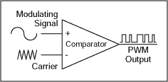
Figure 1. A comparator configured as shown produces a PWM output.
In Figure 2, an op amp generates the triangular waveform and a comparator produces the PWM output signal. Waveforms from this circuit and the relevant equations are shown in Figure 3.
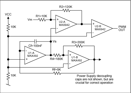
Figure 2. The triangular wave in this basic configuration is produced by a dual op amp (U1), and the PWM signal is produced by a dual comparator (U2).
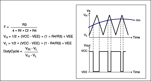
Figure 3. These waveforms and equations illustrate operation of the circuit in Figure 2.
A MAX492 dual rail-to-rail op amp generates the triangular wave. Rail-to-rail capability is required because the dynamic range of the triangular waveform must be larger than that of the sensor. The integrator circuit (U1-A) generates a positive- or negative-going ramp with slope determined by Rf and Cf. The comparator stage (U1-B) reverses the slope of the ramp, and the triangular-waveform frequency is given by the equation in figure 3. For the component values ​​shown , the ramp frequency and thus the PWM output is about 500Hz. Though not shown in Figures 2 and 4, 0.1µF decoupling capacitors should be included at the supply terminals.
A dual comparator (MAX942) compares the ramp waveform with the sensor's analog voltage. This comparator has the rail-to-rail input range necessary for the application. R1 and R2 provide hysteresis, which insures accuracy for the PWM output in the presence of rapidly changing sensor inputs. U2-A provides the PWM output, and U2-B provides isolation and additional buffering.
In the complete PWM transducer circuit (Figure 4), the MAX1452 signal conditioner generates a ratiometric compensated output for the Wheatstone Bridge, which is then converted to a PWM output. As the MAX1452 output changes with pressure, the PWM-output duty cycle changes accordingly . Note that the MAX1452 can be replaced by any of the analog-output signal-conditioning ASICs mentioned earlier.
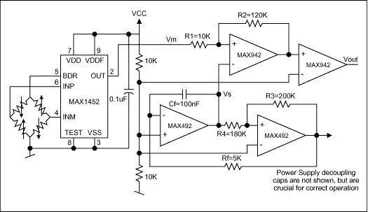
Figure 4. Excitation voltage for the Wheatstone Bridge (above left) is ratiometric with the power supply in this complete PWM transducer circuit.
Sensor compensation requires an accurate measurement of the PWM output's pulse width, and one instrument for that purpose is a frequency counter with pulse-width-measurement option. You can also interface the PWM output to a microcontroller, and use the controller's internal timer to calculate the time interval between low-to-high and high-to-low transitions. Either way, the measured PWM value is used to calculate coefficients needed to program the signal-conditioning IC (a MAX1452, for instance). Sensor Calibration using a PWM OutputThe MAX1452 incorporates four 16-bit digital-to-analog converters (DACs), a temperature sensor, and temperature-indexed coefficient tables suitable for temperature-compensating and linearizing most bridge sensors. The parameters of offset, span, offset TC and span TC can be corrected by loading the four corresponding DACs with unique calibration values. Values ​​loaded in the span and offset DACs are derived from a lookup table. When compared with the 2-poin t compensation algorithm used in the previous generation of signal conditioners, this temperature-driven lookup table adds flexibility and simplifies the calibration process.
Calibration involves loading all four DACs with nominal initial values ​​valid for the transducer family in question. You then set the transducer to temperature T1 and apply maximum pressure. The corresponding PWM output (PWMFS) is measured using one of the methods described above. Next, you measure the PWM output for minimum pressure (PWM0). The PWM span is then PWMSpanT1 = PWMFS -PWM0. Because the required span is normally 80%, the needed span DAC value can be calculated using the expression IdealSpanDACT1 = CurrentSpanDAC × 80% / PWMSpanT1 The Offset DAC is then set to obtain an output with 10% duty cycle.
To obtain values ​​for the span and offset DACs, repeat the above procedure with the transducer at temperature T2. You can add more temperature points (up to 114) for higher accuracy. Programming up to 114 independent 16-bit EEPROM locations enables correction in 1.5 ° C increments over the –40 ° C to + 125 ° C temperature range. (Correction coefficients loaded into the lookup table are linear interpolations between the values ​​recorded for each DAC at each temperature.) Multi-point capability not only enables a simple first -order sensor compensation, it lets you match unusual temperature curves as well. Following this procedure for the above circuit compensates the sensor quickly, efficiently, and within 0.2% of the its inherent repeatability error.
A similar version of this article appeared in the March 2002 issue of Medical Design News magazine.
LED DJ Console Display is a kind of led electronic display screen designed and made according to the customer's specific requirements. DJ Table Led Display Stage can be applied in many fields due to its flexibility of control and combination. It is a bar mark, which is the most distinctive stage facade.
It has an impact on the stage, starts from this moment. It can be widely used in bars, KTV, stage performance and other places.
Characteristics
1. Exquisite effect, smooth transition
2. Assemble and disassemble design, quick and convenient maintenance
3. Innovative unique creation, bar vision 3D design concept
LED DJ Console Display
LED DJ Console Display, Fantasy LED DJ Console Display, Video LED DJ Console Display, LED Honeycomb DJ Console Display
Shenzhen Priva Tech Co., Ltd. , https://www.privaled.com