Schematic diagram of variable capacitance diode frequency modulation circuit
The easiest and most commonly used method is to use the characteristics of varactor diodes to directly generate FM waves. Its principle circuit is shown in Figure 6-1.
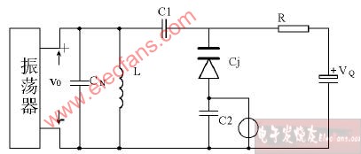
The varactor diode Cj is connected to both ends of the LCN circuit through the coupling capacitor C1 to form a part of the total capacitance of the oscillation circuit. Therefore, the total capacitance C of the oscillating circuit is:
C = CN + Cj (6-3)
The oscillation frequency is:

The reverse bias applied to the varactor diode is:
VR = VQ (DC reverse bias) + Ï… (modulated voltage) + Ï… (high frequency oscillation, can be ignored)
The varactor diode is made of the junction capacitance of the PN junction, and exhibits a certain junction capacitance (barrier capacitance) under the action of the reverse bias voltage, and this junction capacitance can sensitively change within a certain range with the reverse bias voltage, and its relationship Weigh
Cj ~ Ï…R curve, as shown in Figure 6-2.
It can be seen from the figure: when the modulation voltage is not added, the junction capacitance corresponding to the DC reverse bias VQ (called VO in the textbook) is
CjΩ (called CO in the textbook). When the reverse bias increases, Cj decreases; when the reverse bias decreases, Cj increases, and its change has a certain nonlinearity. When the modulation voltage is small, it is approximately the linear segment of the Cj ~ vR curve. Linear change, when the modulation voltage is large, the nonlinearity of the curve cannot be ignored, it will give a certain nonlinear distortion to the frequency modulation band.
Let's go back to Figure 6-1 again, and set the modulation voltage to be very small, working in the linear segment of the Cj ~ Ï…R curve, ignoring the effect of high-frequency voltage on the varactor diode.
Let υR = VQ + VQ cosΩt (6-5)
It can be seen from Figure 6-2 (c): the capacitance of the varactor diode changes with Ï…R.
That is: Cj = CjQ — CmcosΩt (6-6)
According to formula (3), the total capacitance of the oscillation circuit at this time is C ′ = CN + Cj = CN + CjQ — CmcosΩt
YLTelecom produces a variety of Network Faceplate, these faceplates are compatible with our keystone jacks. We have 86 type Faceplate , 120 type faceplate, USA Type faceplate,UKtype faceplate, Australian Type Faceplate, French Type Faceplate, and also German Type Faceplate. These faceplate are available with 1 port, 2 port, 3 port, 4 port, 5 port, and 6 port. They are complaint with international standards and with good material. Due to high quality, our faceplate has recognized by international customers for many years.
We are Quality UTP / FTP Network Keystone Jack Plastic Faceplates with Shutter RJ45 Module manufacturers & exporter,we pffer you many type of Faceplate,like Rj45 Faceplate,Telephone Faceplates,86type Face plate.We can promise you the good quality and low price.

Faceplate
Network Faceplate, USB Faceplate, Rj45 Faceplate, Telephone Faceplates
NINGBO YULIANG TELECOM MUNICATIONS EQUIPMENT CO.,LTD. , https://www.yltelecom.com