Life expectancy indicator
The main reason why power GaN lags behind RF GaN is that it takes time to implement the cost reduction strategy used by several vendors. The best known is the switch to a 6-inch silicon substrate and a lower cost plastic package. For power supply designers, it is important to understand the performance improvements that GaN is likely to bring, as well as some degradation mechanisms that can affect the performance of the final product over time.
The Joint Electronic Equipment Engineering Council (JEDEC) certification standard for silicon devices has proven to be a good predictor of product lifetime, but there is currently no equivalent standard for GaN. To use new technologies to mitigate risks, it is prudent to take a look at specific use cases, as well as the environmental limitations of new technologies in application, and to build prototypes that can stress test and monitor for environmental changes. Real-time monitoring of a large number of prototypes presents some interesting challenges, especially when the GaN device voltage is close to 1000V and dv/dts is greater than 200V/ns.
A chart that is often used to determine if a power FET can meet the target application requirements is a Safe Operating Area (SOA) curve. An example is shown in Figure 1.
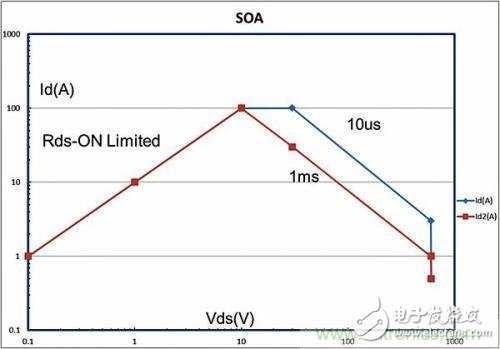
Figure 1. Example of a GaN FET SOA curve, where Rds-On = milliohms
Hard switch design
Power GaN FETs are used in hard switching and resonant designs of several MHz. The zero voltage (ZVS) or zero current (ZCS) topology shown above is several kilowatts. The region where the stress of the SOA curve is the largest is the region where the voltage and current in the upper right corner are the highest. Running a power GaN FET in this hard switching region results in an increase in stress caused by several mechanisms. The easiest to understand is thermal stress. For example, when using an inductive switch test circuit, it is possible to make the device almost zero when the device is turned off, draw a voltage of several hundred volts, and switch the current to almost instantaneously to 10A.
The voltage on the device is multiplied by the current flowing through to obtain instantaneous power dissipation. For this example, it can reach more than 500W in the middle of the conversion. For a typical power GaN device measuring 5mm x 2mm, this value can reach 50W per mm2. So the user does not need to be surprised that this area of ​​the SOA curve only supports short pulses. Due to the thermal limits of the device and the package, the upper right portion of the SOA curve is considered to be a function of pulse width. Due to the thermal time constant seen in the curve, shorter pulses result in less heat dissipation. Enhanced packaging technology can be used to reduce junction-to-ambient thermal resistance from approximately 15 °C/W to 1.2 °C/W. This approach can expand SOA by reducing device heat dissipation.
SOA curve
TI has a range of standard footprint power MOSFETs, DualCoolTM and NexFETsTM. These MOSFETs dissipate heat from the top and bottom of the package and provide 50% higher current than traditional footprint packages. This gives designers the flexibility to use higher currents without the need to increase the size of the terminal. One of the great advantages of GaN FETs compared to silicon FETs is the extremely short switching times that can be achieved. In addition, the reduced capacitance value and the negligible Qrr make the switching losses much lower. When the device is switched, the integer part of the value obtained by multiplying the voltage by the current is the power that the device must consume. Lower losses mean lower device temperatures and greater SOA.
Another important area circled by the SOA curve is limited by Rds-On. In this region, the voltage across the device is the current flowing through the device multiplied by the on-resistance. In the example of the SOA curve shown in Fig. 1, Rds-On is 100 milliohms. The temperature of silicon MOSFETs depends on their Rds-On, which is well known. When the device temperature rises from 25oC to about 100oC, their Rds-On is almost doubled.
Dynamic Rds-On
GaN FETs have a complex Rds-On that is a function of temperature, as well as voltage and time. The dependence of Rds-On on GaN FET on voltage and time is called dynamic Rds-On. In order to predict how a GaN device will operate for a target, it is necessary to monitor the impact of these dynamic Rds-Ons. Similar to the temperature-introduced stress of the SOA curve, the inductive hard-switching stress circuit is more suitable for monitoring Rds-On. This is because many potential device degradations are associated with high frequency switching and electric fields.
Figure 2 is a simple switching circuit in which a method of implementing a circulating current in the upper right quadrant of the SOA and applying stress to the device is presented.
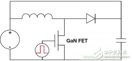
Figure 2. Inductor hard switch test circuit
Wide band gap
KNLE2-63 Residual Current Circuit Breaker With Over Load Protection
KNLE2-63 TWO FUNCTION : MCB AND RCCB FUNCTIONS
leakage breaker is suitable for the leakage protection of the line of AC 50/60Hz, rated voltage single phase 240V, rated current up to 63A. When there is human electricity shock or if the leakage current of the line exceeds the prescribed value, it will automatically cut off the power within 0.1s to protect human safety and prevent the accident due to the current leakage.
leakage breaker can protect against overload and short-circuit. It can be used to protect the line from being overloaded and short-circuited as wellas infrequent changeover of the line in normal situation. It complies with standard of IEC/EN61009-1 and GB16917.1.
KNLE2-63 Residual Current Circuit Breaker,Residual Current Circuit Breaker with Over Load Protection 1p,Residual Current Circuit Breaker with Over Load Protection 2p
Wenzhou Korlen Electric Appliances Co., Ltd. , https://www.zjthermalrelay.com