Since entering the market, CMOS single-supply amplifiers have given designers around the world a significant advantage. The main factor affecting the total harmonic distortion + noise (THD+N) characteristics of the dual power amplifier is the input noise and output stage crossover distortion. The THD+N performance of a single-supply amplifier is also derived from the input and output stages of the amplifier. However, the effect of the input stage on THD+N can complicate this specification of a single-supply amplifier.
There are several single-supply amplifier topologies that accept input signals throughout the power supply. In a complementary differential input stage topology, when the amplifier input approaches the negative rail, the PMOS transistor turns on and the NMOS transistor turns off (Figure 1). When the amplifier input is close to the positive rail, the NMOS transistor turns on and the PMOS transistor turns off.
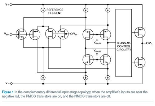
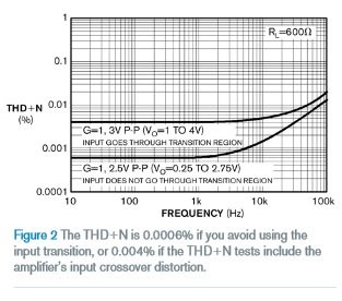
This design topology can dramatically vary the amplifier offset voltage over the entire common-mode input range. In the input region close to ground, the offset error of the PMOS transistor dominates. In areas close to the positive supply, the NMOS transistor pair becomes the dominant offset error. When the amplifier input passes through these two areas, both pairs will turn on. The result is that the input offset voltage varies between the two stages. When both the PMOS and NMOS transistors are turned on, the common mode voltage region is approximately 400mV. This cross-distortion affects the THD of the amplifier. If the complementary input amplifier is configured in a non-inverting configuration, the input crossover distortion affects the amplifier's THD+N performance. For example, in Figure 2, THD+N is 0.0006% if no input conversion is used. If the THD+N test contains the input crossover distortion of the amplifier, THD+N is 0.004%. You can avoid cross-over distortion of this type of amplifier by using an inverting configuration.
Another major factor in generating THD+N may be the output stage of the op amp. The output stage of a single-supply amplifier typically has an AB topology. As the output signal sweeps from one rail to another, the output stage also exhibits cross-over distortion similar to the input stage, at which point the output stage switches between transistors. In general, the THD of the amplifier can be reduced by the large quiescent current of the output stage. The input noise of the amplifier is another factor contributing to THD+N. High input noise, high closed-loop gain, or both, increase the overall THD+N level of the amplifier.
To optimize the THD+N performance of a complementary input single-supply amplifier, the amplifier can be placed in an inverting gain configuration with low closed-loop gain. If the system needs to configure the amplifier as a non-inverting buffer, it is better to use an amplifier with a single differential input stage and charge pump.
FPGA technical data collection - those years, we are crazy about FPGA design
Rechargeable Handheld Vacuum cleaner: This Mini Vacuum Cleaner can be used for cleaning hidden dirty of notebook keyboard, printer, pet food, office, kitchen table, or other small household appliances.
Car mini vacuum cleaner: This Usb Vacuum cleaner can be used for cleaning car vent, dashboard, storage cabinet, sand, dust, paper, food debris, and so on.
Rechargeable wireless vacuum cleaner: this vacuum cleaner power supplied by usb port, which is very easy and convenient to use and store.
Easy to use: this mini vacuum cleaners` filter can be washed by water. Just open the dust pot and take it out, then wash it clean and use it again after it dry.
Cordless Vacuum Cleaner,Cordless Mini Vacuum,Cordless Car Vacuum,Rechargeable Handheld Vacuum
SHENZHEN HONK ELECTRONIC CO., LTD , https://www.honktech.com