What is the PM drive mode?
The passive address drive mode connects the anode of the LED pixels of each column in the array to the Data Current Source, and connects the cathode of each row of LED pixels to the line scan. Line (Scan Line). When a particular Y-th column scan line and X-th line scan line are gated, the LED pixels at the intersection (X, Y) are illuminated. The entire screen can be displayed in a high-speed point-by-point scan in this way, as shown in Figure 1.
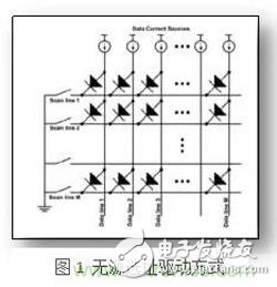
This scanning method is simple in structure and relatively easy to implement.
However, the shortcoming is that the wiring is complicated (requires X+Y root connection), the parasitic resistance and capacitance are large, resulting in low efficiency, and the pixel illumination time is short (1 field/XY), resulting in low effective brightness, easy crosstalk between pixels, and The frequency of the scanning signal is high.
Another optimized passive location driving method is to add a latch in the column scanning portion, and its function is to store the column scanning signals (Y1, Y2 ... Yn) of all pixels in the Xth row at a certain time in advance in the latch. In the device. When the Xth line is gated, the above Y1-Yn signals are simultaneously loaded onto the pixel [3]. This driving method can reduce the column drive signal frequency and increase the brightness and quality of the display screen. However, it still cannot overcome the inherent defects of the passive location selection driving method: the connection is complicated, the crosstalk is easy, and the pixel strobe signal cannot be saved. The active location-driven approach provides a good solution to the above difficulties.
What is the AM drive mode?
In the active addressing drive circuit, each Micro-LED pixel has its own independent drive circuit, and the drive current is provided by the drive transistor. The basic active matrix driver circuit is a two-transistor single-capacitor (2T1C: 2 Transistor 1 Capacitor) circuit, as shown in Figure 2.
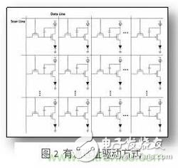
At least two transistors are used in each pixel circuit to control the output current, and T1 is a gate transistor for controlling the on or off of the pixel circuit. T2 drives a transistor that is connected to a voltage source and provides a stable current to the Micro-LED during a frame time. There is also a storage capacitor C1 in the circuit to store the data signal (Vdata). When the scanning signal pulse of the pixel unit ends, the storage capacitor can still maintain the voltage of the gate of the driving transistor T2, thereby continuously driving the current for the Micro-LED pixel until the end of the frame.
The 2T1C driver circuit is only a basic pixel circuit structure of the active-addressed Micro-LED, which is simple in structure and easy to implement. However, since the essence is a voltage controlled current source (VCCS), and the Micro-LED pixel is a current type device, it is difficult to control the display gradation.
What is a "semi-active" location-driven approach? Another thing that needs to be mentioned is a "semi-active" location-driven approach [6]. This driving method uses a single transistor as a driving circuit of the Micro-LED pixel (as shown in FIG. 3), so that crosstalk between pixels can be well avoided.

Compared with passive location, the three major drive modes have obvious advantages, and are more suitable for current-driven light-emitting devices such as Micro-LED. The detailed analysis is as follows:
1 The active location of the drive is more powerful, enabling a larger area of ​​drive. The drive capability of passive location is affected by the performance of the external integrated circuit drive, and the drive area is limited in resolution.
2 Active location has better brightness uniformity and contrast. In the passive addressing mode, the brightness of each pixel is affected by the number of pixels illuminated by this column due to the limited driving capability of the external driving integrated circuit. In general, the same column of Micro-LED pixels share the drive current of one or more output pins of an external drive integrated circuit. Therefore, when the number of pixels illuminated in the two columns is different, the driving current applied to each LED pixel will be different, and the brightness of different columns will be very different. This problem will be more seriously reflected in large-area display applications, such as LED TVs and LED large screens. At the same time, as the number of rows and columns increases, this problem will become more severe.
3 Active addressing enables low power consumption and high efficiency. Large-area display applications require relatively large pixel densities, so the electrode size must be reduced as much as possible, and the voltage required to drive the display will increase dramatically, and a large amount of power will be lost on the row and column scan lines. This leads to inefficiency.
4 High independent controllability. In passive location, a higher drive voltage also introduces a second problem, namely crosstalk, that is, in a passively addressed LED array, the drive current theoretically passes only from selected LED pixels, but Other pixels around will be affected by the current pulse, which will ultimately degrade the display quality. The active location method avoids this phenomenon well by a pixel circuit composed of a gate transistor and a drive transistor.
5 higher resolution. The active location drive is more suitable for high PPI high resolution Micro-LED displays.
The third "semi-active" driver can better avoid crosstalk between pixels, but because there is no storage capacitor in its pixel circuit, and the drive current signal of each column needs to be separately modulated, it can not fully reach the above column. All the advantages of the active location-driven approach.
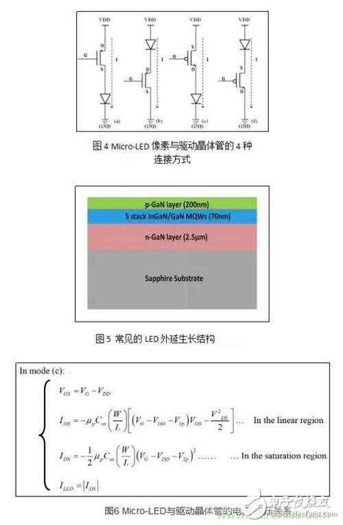
Taking a blue-light micro-LED epitaxially grown on a sapphire substrate as an example, the pixel and the driving transistor T2 are connected in four ways as shown in FIG. However, since the LED epitaxial growth structure is p-type gallium nitride (GaN) on the outermost surface and n-type gallium nitride on the bottom layer, as shown in FIG. From the perspective of the preparation process, it is reasonable to connect the output end of the driving transistor with the p-electrode of the Micro-LED pixel, that is, (a) and (c) in FIG.
The micro-LED pixel in Fig. 4(a) is connected to the source of the N-type driving transistor. The non-uniformity of the electrical characteristics of the Micro-LED caused by the epitaxial growth, the preparation process, and the unevenness of the device aging will directly affect the VGS of the driving transistor, resulting in unevenness of the displayed image. The micro-LED pixel in Fig. 4(c) is connected to the drain of the P-type driving transistor, which can avoid the above influence, and its current-voltage relationship is shown in Fig. 6. Therefore, it is suitable to have a P-tube pixel circuit to drive the Micro-LED.
Maskking(Shenzhen) Technology CO., LTD , https://www.szdisposableecigs.com