introduction
This article refers to the address: http://
The on-board switching power supply is a kind of DC-DC converter, which is different from the ordinary communication power supply. The special use environment requires the power converter to adapt to the high and low temperature environment of -25 to 50 °C, and can prevent the car from running at high speed. The surge of the generator to the power supply and the excessive inrush current directly damage the power supply. At the same time, the design of the on-board switching power supply is limited by the battery power supply, and the low-cost linear power supply cannot be used. Because the switch has the advantages of high power efficiency, small size and light weight, it is widely used. This article uses the switch conversion method.
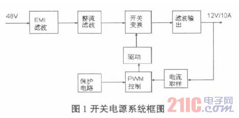
1 48 V~12 V/10 A vehicle switching power supply solution
The vehicle-mounted switching power supply designed in this paper mainly includes two main bodies: the main circuit and the control circuit. The overall block diagram of the system is shown in Figure 1. The main circuit uses a push-pull converter and the control chip is UC3846. The following is a description of the main circuit.
1.1 Input circuit design
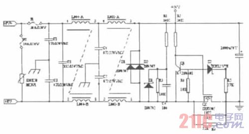
In the DC/DC conversion, the current and voltage values ​​of the switching tube rise and fall rapidly, and the current of the inductor voltage and the capacitor also changes rapidly, which constitute an electromagnetic interference source (EMI). In order to reduce interference, it is necessary to add a filter to the input of the power supply. It consists of C1, C2, C3, C4, C5 and L004, L001 shown in Figure 2.
The vehicle power supply is used in the car and may be subjected to large transient high voltage. The transient overvoltage protection circuit must be added to the input stage. This function is implemented by the varistor S20K60 in Figure 2. At the same time, considering that when the power is turned on, the power supply may have a large inrush current. A resistor must be connected to the input terminal to suppress the surge. As shown in Figure 2, R6, when the converter works normally, the FET Q2's gate current reaches the turn-on current to turn Q2 on, and R6 is shorted at both ends, avoiding excessive power consumption on the resistor. The field effect transistor is IRF3205 (VDSS=55 V ID=110 A RDS(on)=8.0 mΩ). In order to avoid the polarity of the battery connected during installation and damage the converter, the diodes D1 and D2 are connected in parallel on the input stage.
1.2 Design of DC conversion part
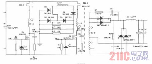
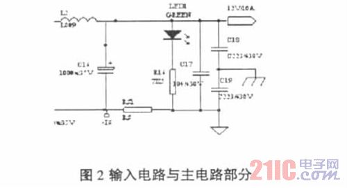
The DC conversion section is the main part of the switching power supply. The switching power supply designed in this paper adopts push-pull type, Q3 and Q4 are power tubes, TR1 is high-frequency transformer, D7, D8, C14~C19, L1, L2 are high-frequency rectifier circuits, and C10 and R4 are switching tubes. Buffer circuit. Q7~Q10 are FET drive circuits.
1.3 Hardware design of switching power supply control circuit
The control circuit adopts UC3846, which is a double-ended output current-controlled pulse width modulator chip. Its pin 1 is the current limit level setting terminal; pin 2 is the reference voltage output terminal; and pin 3 is the current detecting amplifier. Inverting input; pin 4 is the non-inverting input of the current sense amplifier; pin 5 is the non-inverting input of the error amplifier; pin 6 is the inverting input of the error amplifier; pin 7 is the error amplifier feedback compensation; pin 8 is the oscillator External capacitor terminal; pin 9 is the external resistor terminal of the oscillator; pin 10 is the synchronous terminal; pin 11 is the A output terminal of the PWM pulse; pin 12 is the ground; pin 13 is the collector power terminal; and pin 14 is the PWM pulse. B output; pin 15 is the control power input; pin 16 is the closed end.
When the differential current sense amplifier detects the switch current instead of the inductor current, the detection current will have a large peak leading edge due to the parasitic capacitance discharge of the switch tube, which may cause the current detection latch and the PWM circuit to malfunction, so it should be The current detecting input terminal is provided with a filtering circuit. The frequency of the oscillator is determined by the 8-pin external capacitor and the 9-pin external resistor, and the output frequency formula determines:

The current detection input signal is measured by the transformer L014, and then converted into a voltage signal by D3 to D6 and R6 to R8. The current-sampling amplifier output is limited to 3.5 V by the internal circuit, so the maximum voltage input to the current measurement signal should be less than 1.2 V.
Resistors R27 and R29, VR2, and R31 sample the output voltage and compare it with the reference voltage, VREF4, and the op amp, U4B (LM2904N), adjusts the error signal for PI. When the output voltage is too high, the output of the op amp also becomes larger, the diode D12 is turned on, and the current flowing through the transistor Q6 becomes larger, and the diode illuminating intensity of the optocoupler device DT2 becomes stronger, and the current flowing on the triode on the optocoupler device When it becomes larger, the error amplifier feedback compensation terminal current input to the chip UC3846 becomes larger, and the pulse width at the output end of the chip becomes shorter. Reduce the output voltage. This achieves the effect of stable output voltage.
The op amp U4A and its peripheral circuitry form a current limit. The capacitors C25 and R26 at the two inputs of the op amp form the inertia link. When the output current is greater than 10 A, D11 turns on, affecting the intensity of the photocoupler DT2, thus changing the output duty cycle.
2 Experimental results
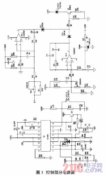
According to the above idea, the switching power supply control circuit shown in Figure 3 is designed. The working waveforms under different conditions were tested and tested under various extreme environments. The experimental results show that the power supply is designed reasonably and can fully meet the requirements of the vehicle environment.
3 Conclusion
With the rapid development of China's economy, the automotive industry is growing stronger. On-board switching power supplies will be widely used as an important electronic device, and the demand for on-board switching power supplies will increase. This design is based on a common power supply that converts a voltage of 48 V to 12 V. The experiment proves that the design is reliable.
The DVD Player is a device that can play DVD discs produced under both the DVD-Video and DVD-Audiotechnical standards. This Media Player will also play audio CDs. This Portable DVD players are connected to a television to watch the DVD content, which could be a movie, a recorded TV show, or other content. We have about 20 years experiences to product this Portable DVD Player With USB, and we also support custom manufacturing, we can offer Hd Video Player OEM/ODM service. Expect traditional DVD Players, we are also manufacture updated version of DVD Player: portable DVD Player and portable video players. Look forward to cooperation with you.


DVD Player
Portable Dvd Player,Usb Portable Dvd Player,Portable Dvd Player With Usb,Portable Dvd Player With Tv Tuner And Radio
Shenzhen New Wonderful Technology Co., Ltd. , https://www.sznewwonderful.com