Binary Phase Shift Keying (BPSK), also known as biphasic modulation, is a fundamental and widely used digital modulation technique. It is favored for its simplicity and effectiveness, especially in scenarios where signal strength is low. The constellation points of BPSK are maximally separated, which enhances reliability in weak signal conditions. Additionally, BPSK offers good spread spectrum capabilities, making it suitable for a variety of applications such as weak signal communication, spread spectrum systems, ranging, and radar [1].
The LTC5548 is essentially a passive, double-balanced mixer with a DC-coupled IF port. When used as a BPSK modulator (as shown in Figure 1), the mixer does not perform frequency conversion, meaning the modulator’s operating frequency range is constrained by the frequency capabilities of both the LO and RF ports. Figure 2 illustrates the test setup for the BPSK modulator. A high-quality vector signal generator with a differential output is used to produce the baseband waveform.
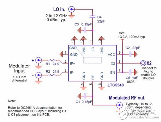
**Figure 1.** RF mixer resistors R1 and R2 are configured as BPSK modulators, each with a 50Ω IF input, ideal for use with modern laboratory equipment.
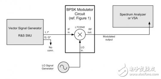
**Figure 2.** Test setup for the BPSK modulator.
**Modulator IF Input Signal**
The differential IF input of the LTC5548 must meet specific drive level requirements to ensure proper operation. The signal should always be balanced, with a common-mode voltage of 0V. Typically, the drive level for each IF pin should be ±0.1V DC (0.2V peak-to-peak). However, the peak signal should not exceed ±0.2V (0.4V pp), and the absolute maximum rating is ±0.3V. Exceeding this limit can lead to unwanted spectral distortion at the RF output.
In most applications, minimizing LO leakage is crucial. This means that the DC offset on the IF input should be as close to zero as possible. While DC offset adjustment can help reduce LO leakage, it cannot eliminate it entirely due to phase differences. Therefore, careful calibration is necessary to achieve optimal performance.
Figure 3 shows the voltages on the IF+ and IF- pins, forming the differential IF input signal. The test circuit corresponds to the configuration in Figure 1. The signal is a balanced waveform centered around 0V and complies with the specified drive levels.
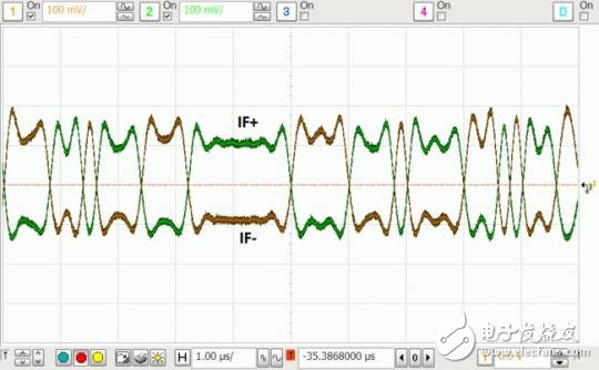
**Figure 3.** Typical modulator drive waveform measured at the IF+ and IF- input pins. Symbol rate = data rate = 5 Mbps.
Zooke Connectors Co., Ltd. , https://www.zooke.com