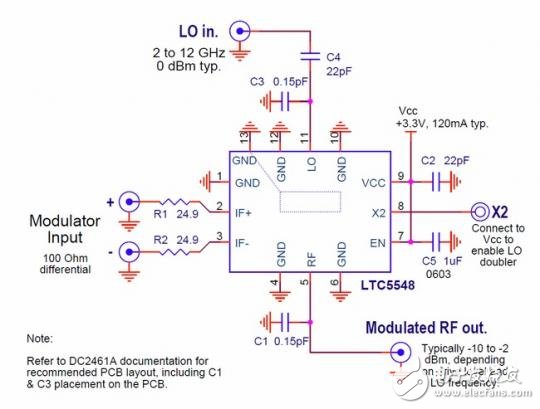
Figure 1. RF mixer resistors R1 and R2 are used as BPSK modulators, each with an IF input of 50Ω, suitable for modern laboratory test equipment.
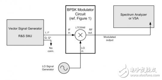
Figure 2. Test setup for the BPSK modulator
Modulator IF Input Signal
The baseband drive level for the LTC5548’s DC-coupled IF input must meet specific requirements:
- The drive must be differential (balanced) with a common-mode voltage of 0.0V.
- The typical drive level for each IF pin is ±0.1V continuous (0.2V peak-to-peak).
- The peak drive level should not exceed ±0.2V (0.4V pp).
- The absolute maximum rating for each IF pin is ±0.3V. However, exceeding this can lead to significant spectral distortion at the RF output.
In most applications, low LO leakage is essential. This means the DC offset on the IF input pins should be close to zero volts. Although DC offset adjustment can help reduce LO leakage, it cannot completely eliminate it due to phase differences in the LO signal.
Figure 3 shows the voltages at the IF+ and IF- pins that form the differential IF input signal. The test circuit is based on the configuration in Figure 1. The signal is a balanced waveform centered around 0V and meets all the specified drive level criteria.
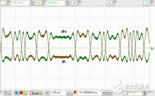
Figure 3. Typical modulator drive waveform measured at the IF+ and IF- input pins. Symbol rate = data rate = 5 Mbps.
Zooke Connectors Co., Ltd. , https://www.zooke.com