1 Introduction
Compared with ordinary light sources, high-power LEDs have the advantages of power saving, long life and fast response time. They are widely used in urban landscapes, LCD backlights, traffic signs, automotive taillights and advertising signs. The active area of ​​the LED chip is small, and the operating current is large, resulting in a high operating temperature of the LED chip. As the junction temperature rises, the LED output optical power is reduced, the chip is accelerated, and the device life is shortened. As the junction temperature rises, the wavelength of the LED will also “red shift†(the visual effects of the orange-red and amber LED color shifts are more pronounced). If you want to take into account the adverse effects of color drift in practical applications, thermal design also limits the maximum junction temperature.
The heat of the chip is conducted to the heat sink through the internal heat path, and the heat sink radiates heat through the air convection or outward radiation. In the high-power LED heat dissipation channel, the metal core circuit board (MCPCB) is the key link connecting the internal and external heat dissipation paths. It has at least the following functions: (1) the heat dissipation channel of the L ED chip; (2) the electrical connection of the LED chip; 3) Physical support of the LED chip.
The substrate material of high-power LEDs must have high electrical insulation properties, high stability, high thermal conductivity, thermal expansion coefficient similar to that of the chip, and flatness and high strength. A small number of metals or alloys can meet the requirements of high thermal conductivity and low expansion coefficient. In order to ensure electrical insulation, a polymer polymer dielectric film is required, the thermal conductivity is usually low, and the performance at high temperatures is deteriorated. Under the premise of satisfying performance and reliability, ceramic material, ceramic film or semiconductor material has unsatisfactory LD substrate materials used for semiconductor illumination from the material itself or the comprehensive cost. Lumileds' Luxeon series of high-power LEDs [3] are the first to use thermal path and electrical path separation in their class of LEDs, which greatly reduces thermal resistance and allows more heat to be released from the die. Lumileds' LED design is groundbreaking. This paper analyzes the design method of Lumileds LED package, analyzes the structure and heat dissipation principle of general high-power LED package, and finally introduces a new type of low-cost MCPCB package material for this type of LED.
2 structure of high power LED and its heat dissipation principle
Lumileds' power LEDs are flip-chip mode with a silicon carrier as the heat sink. While the Zener diode integrated in the silicon heat sink provides electrostatic protection, this design also reduces the impact of thermal expansion coefficient mismatch (silicon and sapphire substrates have similar thermal expansion coefficients). In addition, the silicon material and the solder ball also act as a stress absorber to further alleviate the thermal expansion effect. The solder ball is adhered with a silicon carrier to bond the LED chip tightly to the silicon carrier, and then connected to the lead frame via a wire. The smooth silicon surface has a highly reflective aluminum metal layer. The soldered surface of the LED is typically gold coated to provide optimum heat transfer and bond strength between the chip and the lead frame and copper heat sink. Figure 1 is a schematic diagram of the package structure of Lumileds' Luxeon series LEDs.
The silicon used is very thin, so that the maximum heat transfer performance can be achieved, so that the high heat of the LED is quickly transmitted to the heat sink. Among the various Luxeon products, a primary heat sink (Slug) (about 1.5 mm thick) is attached to the MCPCB by epoxy glue. The MCPCB ensures electrical interconnection and is also the interface to the second stage heat sink. In the absence of a second-stage aluminum heat sink, LE D can also operate at room temperature, but MCPCB can easily reach 7O °C. Although the multi-stage heat sink adds a little thermal resistance, it greatly expands the heat dissipation surface (the heat sink in the inner channel is often called the thermal diffusion layer and should have a high thermal conductivity in all three dimensions). Therefore, the convection heat dissipation and the radiation heat dissipation are greatly enhanced, and the heat dissipation capability of the entire system is improved.
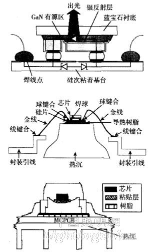
Figure 1 Schematic diagram of Lumileds LED package structure
Another aspect that limits the maximum junction temperature is the maximum allowable thermal stress limit between the silicon carrier and the chip due to the difference in expansion coefficients. In most cases, the high-power LED chip is mounted on the MCPC B through a submount or heat spreader transition, and the MCPCB is placed on the aluminum heat sink. The smooth surfaces of the two are usually fastened with screws or springs and glued with thermal paste. To minimize the interface thermal resistance. Major semiconductor lighting companies, such as Lum ileds, Nichia, Cree, Osram, UOE, Toyota Synthetic, Lamina, etc., have adopted metal core substrates with similar structures. UOE uses a steel core enamel (porcelain / steel core). OSRAM introduced the single-chip "Golden Dragon" series L ED in 2003. Its structural feature is that the heat sink is in direct contact with the metal circuit board. It has good heat dissipation performance and the input power can reach 1 W. The chip uses infrared or reflow soldering. Soldering on a copper alloy heat spreader, the thermal diffusion layer is then soldered to the PC B plate of the aluminum core. The dielectric layer on the surface of the aluminum core is a heat-enhancing polymer with a thermal conductivity of up to 1.3 W/(m·K). Figure 2 is a schematic diagram of the packaging structure of the Golden Dragon.
Lamina Ceramicsl's multilayer low-temperature co-fired ceramic (LTCC-M) multilayer printed circuit board manufacturing technology (shown in Figure 3) achieves a breakthrough in thermal conductivity of LED packages. Multi-layer ceramics are sintered on copper-copper-copper (CuMoCu) metal by low-temperature sintering, and the co-firing shrinkage is reduced to about 0.1%, which is far lower than 12.7% to 15% of the standard LTCC and HTCC processes. The molybdenum-copper composite has a thermal expansion coefficient similar to that of the chip, and the ceramic layer has a high dielectric property, and the LED chip can be directly mounted on the metal plate layer. The thermal conductivity of the metal plate layer is about 17 OW/(m·° C.), and the thermal conductivity of the LT CC is 2 to 5 W/(m·° C.). Capacitors and resistors can be added to the ceramic layer for great convenience in application design. Excellent thermal conductivity allows Lamina Ceramics to align multiple LED illuminating points at high densities, resulting in exceptionally high light in a small area. In February 2005, on an array of approximately 30 cm2, with 1120 LEDs (RGB), 1400W of electric drive, 28000 lm of luminous flux was obtained.
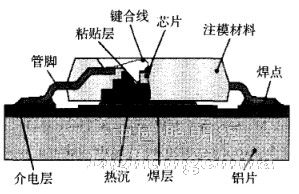
Figure 2 Schematic diagram of Golden Dragon structure
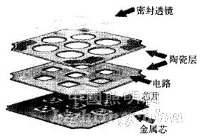
Figure 3 Schematic diagram of the package structure of Lamina LED