In recent years, with the rapid development of LED production technology, its brightness and life extension have been extended, and production costs have been greatly reduced, rapidly expanding the LED application market, such as consumer products, signal systems and general lighting, so its global market scale growing up very fast. In 2003, the global LED market was about 4.48 billion US dollars (high-brightness LED market was about 2.7 billion US dollars), which was 17.3% higher than that in 2002 (the high-brightness LED market grew 47%), and the mobile phone market continued to grow. In 2004, there was still a 14.0% growth rate.
At present, white LEDs used in backlights such as mobile phones, digital cameras, and PDAs are formed by using a blue single chip and YAG fluorescent light. With the application of mobile phone flash, large and medium size (NB, LCD-TV, etc.) display light source modules and special-purpose lighting systems, the application has gradually increased. In the end, it will be extended to use in general lighting system equipment, and the high-power LED market using white LED technology will appear one after another. In terms of technology, the biggest challenge now is to enhance and maintain brightness. If the heat dissipation capacity is enhanced, the market has great potential.
ASM has more than 20 years of experience in R&D and production of automated optoelectronic component packaging equipment. There are many ways to improve LED brightness in the industry, from chip and package design to packaging technology to improve heat dissipation and increase luminous efficiency. . In this article, the latest developments and results of the LED packaging process are summarized and discussed.
Chip design
From the evolution of the chip, it is found that major LED manufacturers continue to improve on the upstream epitaxial technology, such as using different electrode designs to control the current density, using ITO thin film technology to make the current distribution through the LEDs evenly distributed, so that the LED chip is in the structure. The most photons are produced as much as possible. Then use a variety of different methods to extract each photon emitted by the LED, such as the production of chips of different shapes; use the periphery of the chip to effectively control the light refraction to improve the light extraction efficiency of the LED, and develop a single chip surface size (> 2mm2) to increase the illumination Area, more use of rough surface to increase the penetration of light and so on. There are some high-brightness LED chips on which the positions of the two electrodes of pn are close to each other, which improves the luminous efficiency and heat dissipation capability of the chip. Recently, the production of high-power LEDs has been to remove the LED epitaxial wafer from the GaAs or GaN long crystal substrate and bond it to another using the newly improved laser lift-off and metal bonding technology. On metal substrates or other materials with high reflectivity and high thermal conductivity, it helps high-power LEDs to improve light extraction efficiency and heat dissipation.
Package design
After years of development, vertical LED lights (φ3mm, φ5mm) and SMD lamps (surface mount LEDs) have evolved into a standard product model. However, with the development and needs of the chip, we have developed a package design that meets high power. In order to reduce manufacturing costs by using automated assembly technology, high-power SMD lamps have emerged. Moreover, driven by the rapid market of portable consumer products, the design of high-power LED package volume is smaller and thinner to provide a wider product design space.
In order to maintain the brightness of the finished product after packaging, a new modified high-power SMD device with a cup-shaped reflecting surface helps to reflect all the light out of the package to increase the output lumen. The LED optical lens on the LED is covered, and the material is changed to use Silicon sealing, instead of the epoxy resin (Epoxy), so that the package can maintain a certain durability.
Packaging process and solution
The main purpose of the semiconductor package is to ensure the correct electrical and mechanical interconnection between the semiconductor chip and the underlying circuit, and to protect the chip from mechanical, thermal, humid and other external impacts. When selecting the packaging method, materials, and operating the machine, factors such as the shape of the LED epitaxial, electrical/mechanical characteristics, and the accuracy of the die attach must be considered. Due to the optical properties of LEDs, packaging must also be considered and ensured in optical properties.
Whether it is a vertical LED or SMD package, a high-precision die bonder must be selected. The accuracy of the placement of the LED chip in the package directly affects the luminous performance of the package. As shown in Figure 1, if the position of the chip in the reflector cup is deviated, the light is not completely reflected, which affects the brightness of the finished product. However, if a solid crystal machine has an advanced pre-image identification system (PRSystem), it can be precisely welded to a predetermined position in the reflector cup despite the poor quality lead frame.
Generally, low-power LED devices (such as the illumination of pointing devices and mobile phone keyboards) are mainly solid crystals with silver paste. However, since the silver paste itself cannot withstand high temperatures, while the brightness is increased, heat is generated, which affects the product. In order to obtain high-quality and high-power LEDs, a new die-hardening process has been developed, one of which is to use eutectic soldering technology to solder the chip to a heat sink (soubmount) or heat sink (heatsink). The whole chip is connected to the heat dissipating substrate and soldered to the package device, so that the heat dissipation capability of the device can be enhanced, and the luminous power is relatively increased. As for the substrate material, silicon (Silicon), copper (Copper) and ceramic (Ceramic) are commonly used heat-dissipating substrate materials.
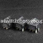
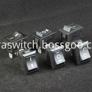
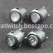
Kara offers a wide range of illuminated and non-illuminated Rocker Switches.In this series,Rated current 6A,10A,16A,Ranging from 1 to 6 poles,with many styles of colors and functions. Certifications include UL, CSA, TUV, CE, and more.
Why choose us?
1)As a manufacture, all of our switch parts are made by our own factory in Ningbo. So, price is competitive.
2)We have our own UL testing lab in Taiwan, so quality can be guaranteed.
3) We can provide you with different types of rotary switches for your selection.
4) Various operating force,height and colour for one switch for your choice.
5) Safety, on-time delivery, excellent quality with competitive price.
6) MOQ: 1000pcs,mixed order acceptable, welcome trial order.
7) OEM and ODM professional design.
8) We can provide free samples for your test.


Small-Sized Rocker Switches,Round Rocker Switch,Small Rocker Switch,Mini Rocker Switch
Ningbo Kara Electronic Co.,Ltd. , http://www.kara-switch.com