Many of today's embedded industrial and automotive systems are based on 8-bit or 16-bit microcontroller architectures. With the introduction of new low-power 32-bit architectures, these applications are likely to achieve higher performance, accuracy and efficiency. In addition, increased processing power helps to enable differentiated functionality for new products, including advanced control algorithms, GUI displays, voice control, and next-generation interfaces such as capacitive touch sensing.
This article refers to the address: http://
For example, in many industrial applications, motor efficiency is one of the main factors affecting power consumption. Motor efficiency can be improved with advanced control algorithms, but these algorithms require higher performance microcontrollers. On the other hand, communication speed also affects efficiency, because the higher the communication speed, the more information the system can collect from the sensor, while identifying events and taking action more quickly.
The past 32-bit architecture conversion has been delayed for many reasons, such as the high cost of the microcontroller, does not support 5V I / O and so on. Now, with Atmel's AVR® UC3C 32-bit microcontroller with an industrial-grade microcontroller with a floating-point unit (FPU), these and even other design issues have been Solve the solution. The AVR UC3C integrates a peripheral event system, a high-precision clocking scheme, and high-performance peripherals to improve system performance, reliability, and power efficiency. In addition, the integration of secure Flash, hardware-based security, the ability to connect directly to analog sensors, and configurable software frameworks can greatly accelerate application development. Finally, the AVR UC3C is optimized for the specific requirements of industrial and automotive applications, providing not only 32-bit processing power, but also power consumption equivalent to the level of 8-bit or 16-bit microcontrollers.
32-bit processing performance
The efficiency difference between 32-bit and 8/16-bit systems is quite large. On a 16-bit processor, a normal 32-bit multiply/accumulate operation requires 4 multiplications and 4 additions. Due to the need to access memory to store intermediate results or to release multiple registers, execution efficiency is further reduced and may slow down other operations. Therefore, on a 16 processor, a 32-bit multiplication may take 20 to 40 cycles. The 32-bit UC3C processor only needs a single cycle. In addition, the 32-bit pipeline is wider, so data and instructions are retrieved faster from memory.
The introduction of the integrated FPU also further simplifies application development. When an algorithm is too cycle-intensive or needs to be implemented in a fixed-point format, it takes a significant portion of the product development cycle to find ways to simplify the algorithm and speed up the computation. This type of simplification is often at the expense of accuracy. The use of FPU to implement complex algorithms requires less work, a wider dynamic range, and the highest accuracy. Using 32-bit floating-point instructions to implement complex algorithms can not only improve the accuracy and efficiency of the system, but also greatly accelerate the development process. Floating point technology is useful for a wide range of applications, including robotics, motion control, motor control and audio applications.
Atmel's AVR® UC3C 32-bit microcontroller instruction set is a rich instruction set that combines 16-bit and 32-bit instructions to balance performance and code density with the C compiler. However, the biggest advantage of the UC3C microcontroller is that its architecture is optimized for real-time event management common in embedded systems. The UC3C microcontroller supports a wide range of high precision peripherals and interfaces, such as CAN and LIN for embedded systems, and supports reliable operation over the entire industrial temperature range. The AVR UC3C architecture is designed to minimize processing delays to ensure real-time event processing, as shown in Figure 1, for system reliability and operator safety for microcontrollers.
Figure 1 shows the Atmel AVR UC3C 32-bit microcontroller, a high-performance microcontroller designed with low processing latency to ensure real-time event processing to ensure system reliability and operator safety.
Figure 1 Atmel AVR UC3C 32-bit microcontroller design block diagram
Enhanced processing power can improve application performance in a number of different ways:
Higher Accuracy and Accuracy: Greater processing power allows microcontrollers to support more accurate ADCs and DACs at higher sample rates.
Direct use of analog sensors: The AVR UC3C features a DMA-based ADC, advanced processing capabilities, and an integrated technology that properly manages the precise timing of analog sensors, allowing for more analog sensors than traditional microcontroller architectures.
More advanced algorithms: Implementing more advanced algorithms, such as three-phase motor control and dead-band insertion techniques, can increase system efficiency and reduce system power and cost.
Differences: Greater processing power enables more advanced user interface graphics. For example, many microcontrollers require 4 or 5 chips to implement the capacitive touch function of the system. With the flexible, high-performance AVR UC3C, the capacitive version can be touch implemented in software and can be operated from any I/O pin without external components.
Greater communication bandwidth: The system can share more data, control multiple nodes, and capture higher resolution data. Current 16-bit systems often cannot support a single CAN or Ethernet stack. With a 32-bit architecture with DMA, a single device can act as a multi-interface gateway.
5V I/O standard
As manufacturing processes shrink in size, microcontroller vendors are also responsive to the situation, working to reduce I/O voltages to reduce power consumption and improve stability. Although this voltage reduction is advantageous for many applications such as consumer electronics, it is not suitable for 3.3VI/O because the system in the industrial market requires a longer service life. Therefore, most components in industrial applications are still based on 5V I/O.
32-bit processors have only been providing 3.3VI/O, because they have a larger number of transistors, resulting in smaller geometry in their manufacturing process. To support the large number of 5V-based industrial components on the market, these processors require additional circuitry, including costly level shifters and power supplies, to reduce the 5V I/O to 3.3V for easy connection. Of course, higher processing power is always welcome, but higher costs are not acceptable to the market. It is also impractical to switch to 3.3VI/O and components. Most sensors and other industrial components are based on 5V, so it's much easier and more cost-effective to continue to use 8-bit and 16-bit microcontrollers instead of all the sensors needed for the system.
The unique Atmel® VR3C 32-bit microcontroller is the first industrial-grade microcontroller to support 5V I/O. This result is achieved through more advanced 0.18μm process technology because it supports higher I/O voltage levels in a reliable and cost-effective way. This intrinsic 5V I/O allows the AVR UC3C-based design to take full advantage of the new CPU performance of 32-bit microcontrollers without the need for any complex and expensive voltage conversion devices.
In addition to supporting 5V I/O, the AVR UC3C comes with a wide range of high-performance peripherals to meet the needs of industrial and automotive applications:
ADC: 16 channels, 12 bits, sampling rate up to 1.5Msps; dual sampling and hold capability; built-in calibration; internal and external reference voltage.
DAC: 4 outputs (2 × 2 channels), 12-bit resolution; conversion rate up to 1Msps, 1us settling time; flexible conversion range; 1 continuous output per channel or 2 sample/hold outputs.
Analog Comparator: 4 channels with optional power and speed; optional hysteresis (0V, 20mV and 50mV); flexible input selection and interrupt; combined with window comparison of two comparators.
Timer/Counter: Multiple clock sources (5 internal, 3 external); rich feature set (counter, capture, up/down, PWM); 2 input/output signals per channel; global start control, Achieve synchronous operation.
Quadrature Decoder: Integrated decoder that supports direct motor rotation detection.
Multiple interfaces: Includes a dual 2-wire interface (TWI), master/slave SPI, and a full-featured USART that can be used as an SPI or LIN.
Fully integrated USB: Built-in USB 2.0 transceiver supporting low (1.5Mbps), full (12Mbps) and On-The-Go modes. In addition, the AVR software framework provides production-ready drivers for a variety of USB devices (mass storage, HID, CDC, audio), master devices (mass storage, HID, CDC), and composite functional devices.
Higher system throughput
Peripheral management may have become a major system bottleneck, and the situation is more severe with the number of peripherals and their increasing frequency of operation. In a traditional interrupted system, data arrives at an interface or sensor port, and the CPU must read and store the result before being overwritten by the next data value. Due to the high channel multi-sampling rate, interrupt overhead and data processing consume a significant percentage of the available clock cycles of the processor. As the number of managed peripherals increases, the interrupt latency also increases, introducing jitter and reducing accuracy. In addition, other design issues arise, such as priority interrupt handling that complicates task scheduling.
To facilitate efficient operation of multiple high-performance peripherals, the AVR UC3C architecture employs a peripheral event system that allows peripherals to self-manage and communicate with each other without the intervention of the host processor, as shown in Figure 2. The peripheral event controller independently processes the inter-peripheral signaling of the CPU through an internal communication structure that enables all peripheral interconnects. Instead of triggering an interrupt to inform the CPU to read peripheral or port data, the peripheral can self-manage and pass the data directly to the SRAM store, all without any CPU intervention. From a power point of view, only those conversion function modules are active. During the entire event, the most power-consuming component CPU in the device is released to execute the application code or enter the IDIE mode to save power without having to be active in order to handle high-frequency interrupts.
Figure 2 shows that the peripheral event system allows peripherals to self-manage without the intervention of the host processor. For example, if there is no peripheral event system, the timer will trigger a conversion on an ADC, then pass the result to the DMA and store it in memory, all without any intervention from the CPU. With a peripheral event system, there is no jitter, and when the Atmel AVR is operating at 66 MHz, the response delay is fixed at only 33 ns for three cycles.
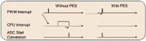
Figure 2 Peripheral event system allows peripherals to self-manage
The response of the peripheral event controller is more deterministic than the CPU-based interrupt-driven event controller. When the 32-bit AVR UC3C is operating at 66MHz, the delay is fixed at three cycles or only 33ns, resulting in jitter-free precise event timing, making data reading and transmission on the ADC and DAC more accurate. This delay is predictable and features that do not require CPU overhead to prevent event omissions or data loss.
To fully observe the functionality of the peripheral event system, consider the CPU load required to manage a single SPI port. If the data transfer between the peripheral and the SRAM is based on an interrupt, the SPI port will trigger an interrupt when it receives the data, then the CPU saves the application context and transfers the data to the appropriate data buffer of the SRAM. Restore the application environment. Even at a low data rate of 1.2 Mbps, managing the SPI port requires 53% of the processor power.
Conversely, if a peripheral event system is used, the USB port will automatically transfer the received data to the DMA. The DMA then automatically stores this data in the appropriate memory buffer, all without any intervention from the CPU. In essence, the use of a peripheral event system eliminates all interrupts associated with peripheral management, leaving more CPU power available to the application.
Peripheral event systems also reduce the overall complexity of real-time system management. Taking a typical three-phase motor control application as an example, this application requires a PWM to drive current using on/off pulse transmission. In the open-loop architecture, two currents must be measured simultaneously to determine the back-EMF to calculate the rotor position. The closed-loop architecture also needs to measure two currents to read the position and orientation data returned by the incremental encoder. In an emergency, the system also needs to perform a hardware failure mechanism to stop the motor. With the Atmel AVR® UC3C 32-bit microcontroller, all of these inputs and outputs can be managed in the background via the peripheral event system.
Industrial and automotive applications require a large number of different clocks to implement the many functions supported by these systems. The AVR UC3C architecture provides multiple clock options, eliminating the need for multiple external clock sources that the system might otherwise need. The clock options offered by the AVR UC3C include three internal RC oscillators (115kHz, 8MHz, and 120MHz) and a phase-locked loop (PLL) for generating high-speed system clocks from 80MHz to 240MHz. Any oscillator can be used as the system's real-time clock (RTC) source, and an external oscillator can be used to provide additional clock frequency.
IP protection
Code protection has become a key design consideration because of the current industry outsourcing and offshoring, and the increasing intellectual property (IP) of software. The three main factors related to IP protection include:
Protection of source and target code: Flash that stores program code must have a locking feature to protect the code from being read or copied. This not only prevents competitors from stealing application code, but also prevents unrecognized offshore manufacturers from copying code and privately manufacturing products for local sales.
Partial locking of the code: Using application code provided by third-party developers can significantly speed up the system development process, especially for applications that rely on proprietary algorithms. Traditional protection mechanisms, such as those that only provide object code, are not sufficient to protect the investment of third parties because they cannot verify the number of times the code is used. Partially locked Flash allows third-party developers to confidently provide proprietary code because the code is already programmed on the microcontroller.
Device Programming Cost: The microcontroller must be programmed before it is installed on the board or in-device programming. Pre-programming techniques present a challenge to logistics because the devices must first be programmed on a reliable facility and shipped to the manufacturing facility. In-device programming techniques add the latest code during the manufacturing phase. One common method of device programming is to utilize the JTAG port of the microcontroller. The disadvantage of this method is that four I/O pins need to be specified for this purpose, and the binary code is exposed when it is transferred between the microcontroller and the board. The alternative is to have the device load the bootloader code at the factory with enough functionality to support an interface such as a USB port. The AVR UC3C comes with a USB drive that supports Device Firmware Upgrade (DFU), allowing the device to be programmed through the system's USB port. This frees the I/O pins and removes the JTAG header from the system BOM.
The Atmel AVR® UC3C 32-bit microcontroller architecture also includes Atmel's FlashVaultTM code protection technology. FlashVault allows on-chip Flash for partial programming and locking, creating secure on-chip memory to protect software IP. The locked portion of Flash cannot be read, copied, or debugged. During development and debugging, FlashVault can also work in a partially unprotected mode to access application code stored in Flash while still protecting third-party code. The boot loader code can also be locked to ensure that the device is always able to reload the application code in the event of a catastrophic software failure.
System security
For industrial and automotive applications, safety is a major consideration because of system failures that can have costly consequences and can even result in operator casualties. In fact, a significant percentage of systems experience clock failures, and the system must have the ability to recover from clock failures, especially for industrial systems where life expectancy is expected to be decades. For example, the motor control system must be able to intelligently shut down the system when a clock failure is detected to protect the motor or operator from catastrophic damage. To this end, the AVR UC3C device can detect the main clock failure and switch to an internal 115kHz RC oscillator. The system can continue to run with the backup clock (while triggering an alarm that the primary clock fails) or perform any necessary shutdown operations to put the system into a fail-safe state.
Another important security feature is the windowed watchdog timer. Microcontrollers typically use a watchdog timer to monitor the system for proper operation. If the application code is corrupted, the watchdog timer will not be started and a software reset will be triggered to warn that the system failed to boot. This mechanism is especially important after a software update to ensure a successful update.
However, there is a problem with the watchdog timer, which is that it is set and activated by software. If the code to set the watchdog timer has never been executed, the fault protection interrupt will not be triggered. The windowed watchdog timer, shown in Figure 3, is a more reliable form of fault detection that defines a narrower watchdog start window. This scheme still requires the timer to be started in software, but there is no abnormality that the watchdog cannot be set because it is set and activated by hardware, and the corrupted application can be prevented from modifying the watchdog configuration. . Thus, the windowed watchdog is always set and activated when the system is powered up, so if the application code is corrupted, the failsafe interrupt will be triggered after the set time.
The purpose of the watchdog timer shown in Figure 3 is to verify that the system is functioning properly by requiring the application to clear the watchdog timer within the set time frame. For the traditional watchdog timer, if the corrupted system resets the watchdog timer, failure detection cannot be performed without first activating it. The windowed watchdog timer is set and activated in hardware when the system is powered up, thus ensuring that system faults are detected.

Figure 3 windowed watchdog timer
The windowed watchdog timer is only activated within a certain time frame. For example, there is an interrupt that should return to the main loop (starting the watchdog timer) after a certain number of cycles have been executed. If the interrupt returns too fast, the interrupt is not executed correctly, so there may be a system problem. For the traditional watchdog timer, this problem is ignored. With the time frame watchdog timer, the timer will be started too fast, triggering a watchdog interrupt.
Accelerated system development
Today, when evaluating a microcontroller architecture, you need to consider not only the hardware capabilities of the device, but also what software libraries and application-ready applications you can use. Designing a complete system from scratch requires a lot of development resources and time. Conversely, using existing software frameworks can speed up time to market and significantly reduce investment in application development.
The Atmel AVR® software framework simplifies system development by supporting a wide range of optimized interface drivers, peripheral firmware and application code, including numerous motor control algorithms, capacitive touch drivers, and advanced digital signal processing algorithms (ie, FFT). , as well as bandpass, Qualcomm and low-pass filters), common audio and image codecs (such as MP3), speech recognition engines, display drivers, CAN/LIN services, and FAT12/16/32 file systems. Utilizing the framework to implement peripheral or interface drivers greatly simplifies firmware development and reduces the time required to port applications on the AVR product line. For example, three UART drivers can be used to support RS-232 and RS-485 interfaces, and can also cover one CAN interface. Similarly, creating a USB drive is as simple as selecting a device class, and the framework provides the corresponding driver code and protocol stack. The framework also includes a complete real-time operating system (freeRTOS) and supports many popular products such as uC-OS/II, embOS, ThreadX and openRTOS. Atmel provides the AVR software framework to customers for free.
Using a broad software framework helps to reduce development time and speed time to market. The AVR software framework provides the industry's broadest selection of production-ready software drivers and libraries, and includes a rich set of sample application complete documentation code. The AVR microcontroller supports real-time tracking for complete visualization of system operation. In addition, AVR microcontrollers are updated quarterly to introduce new features.
The intuitive GUI-style Atmel AVR Studio® development environment allows for quick configuration of drives and interfaces, so that the first prototype can be implemented in minutes rather than months, as shown in Figure 4. Fast and simple peripheral configuration is critical to the industrial market, as the entire design team is able to focus on application development rather than wasting code on another UART drive. AVR Studio is the industry's most comprehensive 8-bit and 32-bit application development environment, providing comprehensive compiler and debugger support for all AVR microcontrollers. Since the peripherals are configured using the AVR software framework, the migration between different AVR devices is truly seamless. AVR Studio is fully integrated with the AVR software framework, both of which are available for free or without benefits.
Figure 4 shows the Atmel AVR Studio development environment, which provides drive and interface firmware for all peripherals. With this approach, the first prototype can be configured in minutes instead of months.
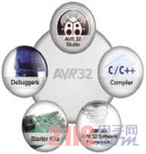
Figure 4 Atmel AVR Studio development environment
Atmel also offers a wide range of hardware-based in-system programming, debugging and evaluation tools. For example, the Atmel AT32UC3C-EK evaluation kit provides out-of-the-box simplicity, providing access to a wide range of features in the Atmel AVR® UC3C 32-bit microcontroller architecture. It has access to every pin and on-chip resource to directly verify the outstanding low-power characteristics of the AVR UC3C in a simple process. The evaluation kit also includes Atmel QTouch® capacitive touch capability, as well as RF4CE, ZigBee, Wi-Fi and Bluetooth plug-ins for wireless connectivity.
The real system design is not to simply combine different chips or subsystems. Today's embedded applications are complex systems that contain many functional components. The conversion to a 32-bit architecture allows the design to be integrated on a single microcontroller that is optimized for high performance, low power, real-time processing and system reliability. In addition, system design can now be completed in a single coordinated environment, speeding up system development and testing.
The AVR UC3C is the industry's first 32-bit processor designed for industrial and automotive applications. UC3C integrates floating-point computing power and peripheral event systems to support 32-bit performance. It provides the performance and processing power to introduce advanced functionality to these systems and create new market opportunities. Combined with the right combination of high-precision peripherals, native 5V I/O, secure flash, and the most complete design environment, combined with production-ready code for motor control, sensor monitoring, and digital signal processing, UC3C is the one that needs real-time reliability. The ideal MCU option for high performance and high efficiency applications.
LED Canopy Light is light-emitting diodes as luminescent materials, mainly used for gas stations, factories, Stadium,Department store and other places, requiring high explosion-proof grade, high safety factor.
Our product features:
1) Philips 3030 LED,MEANWELL Driver,CE, RoHS Certification.
2) Reduce glare, avoid assassination eye, highlight the overall space lighting, improve the overall brightness of the gas station.
3) Low energy consumption design, the maximum energy conservation.
4) Over load protection, over voltage protection, over temperature protection, short circuit protection
5) Long service life, low maintenance and repair rate.
6) Beautiful appearance,Concept of humanized design, embodies the modern industrial lighting fashion aesthetic requirements and human nature full of harmonious ideas, integration.
LED Canopy Light
LED Canopy Light,LED Canopy Lights For Gas Station,LED Canopy Light Fixture,LED Canopy Light Retrofit Kit
Shenzhen Ri Yue Guang Hua Technology Co., Ltd. , http://www.ledlightinside.com