Online upgrade
1. Open Skyworth cool open TV, enter the home page, select "Settings" - "System Upgrade" - "Online Upgrade", if the TV's system has been updated, you will be prompted to discover the new version (as shown below) , If not, it will show "Temporarily no software update";

2. In the dialog box that pops up, the "Cautions" of the upgrade will be given. After careful reading, click "Download". On the top right corner of Cool TV, the system prompt "System Package Downloading" will appear;

3. After the download is complete, click "Upgrade" to enter the upgrade mode. After the upgrade is completed, a dialog box will pop up to indicate that the upgrade is complete. Click OK. After the upgrade is completed, Skyworth Cool TV system will automatically turn off the TV and enter the upgrade status.
Local upgrade
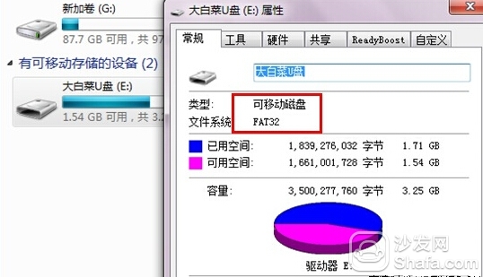
1. Download Skyworth cool TV firmware update package (Before downloading the upgrade package, please make sure that Skyworth cool TV's movement, different movements, upgrade package is different), after downloading copy to U disk (must FAT32 format Processing, readers and mobile hard disks cannot be used, since no decompression is required;
2. Unplug Skyworth Cool to open all connections on the TV, such as external devices, SD cards, VGA cables, etc.
3, to ensure Skyworth cool open TV is not standby, then turn off the power, plug in the U disk (recommended to plug the top USB interface);
4. Turn on the TV, and then enter the "Home Page" - "Settings" - "System Settings" - "System Update" - "Local Upgrade", select OK.

5, Skyworth Cool TV system will restart into the upgrade mode (blue background progress bar) The upgrade process will have about 10 minutes, after the upgrade will automatically restart.

Precautions:
1, please be sure to use FAT32 format U disk upgrade, otherwise it will not be successful upgrade!
2. This upgrade will clear all your data: settings, installed applications and application data.
3, after the upgrade the original download and installation of the application may disappear, please download the installation before the first backup!
4, if you can not find the upgrade package, please replace the U disk or restart the machine and try again.
5, U disk needs to be placed in the file name must be strictly matched, otherwise it will not be able to upgrade because it can not find the specified file.
6 Layer PCB - stackup & prototype & price & manufacturing
What is 6 Layer PCB?
6 layer PCB Board is, in general, a 4 Layer PCB Board with 2 extra signal layers added between the planes. The 6-layer PCB classic stackup includes 4 routing layers (2 outer layers + 2 internal layers) and 2 internal planes (one for ground and the other for power). This enhances the EMI dramatically by offering 2 buried layers for high-speed signals and 2 surface layers for routing low-speed signals. The signal layers should be closed to the adjacent planes.
6 Layer PCB Prototype Fabrication China Manufacturer
Jinghongyi PCB has been committed to the production of multi-layer PCB and Prototype PCB for nearly 10 years. The largest number of multi-layer Printed Circuit Boards for customers are 4-layer, 6-layer, 8-layer, 10 layer, 12 Layer PCB and above. In order to ensure the quality of PCB products, we constantly improve and upgrade the production process. PCB surface treatment technology has hot air leveling(HASL), OSP, electroless nickel, immersion gold, immersion silver, immersion tin and so on.
The Printed Circuit Board is basically composed of the pad, via, solder mask layer, silkscreen layer, copper wire, and other parts. Among them, solder mask refers to the part covered by ink on PCB. Because most PCB uses green ink, the green ink part that can be seen is solder mask. The role of the solder mask in controlling the reflow welding process is very important. In addition to green ink, the welding layer can According to the different needs of customers, and can also be customized in a variety of colors, such as green, blue, black, red, white, yellow, purple. Of course, the price will vary with the color of the solder mask. Green oil is the one with low price and stable quality, which is also the reason why green oil is most used. The price of black oil, red oil, and white oil is almost the same, slightly more expensive than green oil, and the price of rare inks such as yellow and violet oil is the highest. In addition to the color of the solder resist ink, there are also matte and bright, matte ink color.
Based on our very experienced PCB engineer, we can help you in the 6-layer PCB stack up and design as much as possible.
In addition to providing you with 6-layer PCB and prototype manufacturing, we also provide one-stop prototype assembly services, including electronic components procurement, stencil, etc. The turnkey Printed Circuit Board Assembly services make your R&D work easy and time-saving.
6 Layer PCB Stackup and Design
What is PCB stack UP?
PCB Stack up refers to the arrangement of copper and insulation layers that make up PCB before the layout design of circuit board. Although stacking allows you to get more circuits on a single board through various PCB layers, the structure of PCB stacking design has many other advantages:- The PCB layer stack can help you minimize circuit noise and radiation and reduce impedance and crosstalk problems in high-speed PCB layouts.
- A good stacked PCB stack can also help you balance the need for low-cost, efficient manufacturing methods and focus on signal integrity issues.
- Proper PCB stacking can enhance the electromagnetic compatibility of your design.
- For PCB-based applications, stacked PCB configurations are usually good for you.
Why do PCBs stack up?
The irreversible development of modern electronic products has increasingly pushed PCB towards such needs as miniaturization, light weight, high speed, better functionality and reliability, and longer life, which has led to the popularity of multi-layer PCB. Two or more Single Sided PCB and/or Double Sided PCB are stacked together by a combination of semi-solid adhesives called "prepregs" to form multilayer PCBs through reliable predefined interconnections between them. There are three or more conductive layers in a Multilayer PCB , two of which are outside, and one is synthesized in an insulating board. With the increasing complexity and density of PCB, some problems may arise, such as noise.
One of the most important factors to determine the performance of product electromagnetic compatibility (EMC) is to plan the optimal multi-layer stack up. The carefully designed cascade can minimize radiation and prevent the circuit from being disturbed by external noise sources. Good stacked PCB substrates can also reduce signal crosstalk and impedance mismatch. However, poorer stacking may increase EMI radiation, because impedance mismatch will lead to reflection and ringing in the system, which will greatly reduce the performance and reliability of the product. Then, this article will focus on the layer stack definition, design rules and basic considerations.
Most six-layer PCB consist of four signal routing layers and two planes. From an EMC perspective, a 6-layer Printed circuit board is usually better than a 4 Layer PCB board.
6 Layer PCB Stackup

6 layer 1.6 MM standard stackup and thickness

Fig. 1 One of the stackup methods of 6-layer PCB
With six layers available the principle of providing two buried layers for high-speed signals is easily implemented as shown in Fig. 2. This configuration also provides two surface layers for routing low speed signals.

Fig. 2 Less common 6 layer PCB stackup
Not nearly as common, but a good performing stack-up for a six-layer PCB is shown in Fig. 2.

Fig. 3 Another performing six-layer PCB board stackup
Another excellent performing six-layer PCB board stackup is shown in Fig. 4. It provides two buried signal layers and adjacent power and ground planes and satisfies all five objectives. The big disadvantage, however, is that it only has two routing layers -- so it is not often used.

Fig. 4 Another excellent performing six-layer PCB board stackup

6 Layer PCB Stackup for EMI/EMC

EMI/EMC Return Current 6 Layer PCB Issue

EMI/EMC Return Current 6 Layer PCB Solved

Types of 6 PCB stack up-how to choose?
PCB materials and stackup thickness commonly used in multilayer circuit boards.
| 6 Layer Stackup - 0.8mm thickness | ||||||
| layer order | layer name | material type | material description | dielectric constant | thickness | copper weight |
| 1 | top | copper | signal | 0.035mm | 1 oz | |
| 2116 | prepreg | 4.5 | 0.12mm | |||
| 2 | inner 1 | copper | plane | 1 oz | ||
| core | 4.6 | 0.2mm | ||||
| 3 | inner 2 | copper | plane | 1 oz | ||
| 2116 | prepreg | 4.5 | 0.12mm | |||
| 4 | inner 3 | copper | plane | 1 oz | ||
| core | 4.6 | 0.2mm | ||||
| 5 | inner 4 | copper | plane | 1 oz | ||
| 2116 | prepreg | 4.2 | 0.12mm | |||
| 6 | bottom | copper | signal | 0.035mm | 1 oz | |
| Final board thickness: 0.8mm±0.1mm | ||||||
| 6 Layer Stackup - 1.0mm thickness | ||||||
| layer order | layer name | material type | material description | dielectric constant | thickness | copper weight |
| 1 | top | copper | signal | 0.035mm | 1 oz | |
| 2116 | prepreg | 4.5 | 0.12mm | |||
| 2 | inner 1 | copper | plane | 1 oz | ||
| core | 4.6 | 0.3mm | ||||
| 3 | inner 2 | copper | plane | 1 oz | ||
| 2116 | prepreg | 4.5 | 0.12mm | |||
| 4 | inner 3 | copper | plane | 1 oz | ||
| core | 4.6 | 0.3mm | ||||
| 5 | inner 4 | copper | plane | 1 oz | ||
| 2116 | prepreg | 4.2 | 0.12mm | |||
| 6 | bottom | copper | signal | 0.035mm | 1 oz | |
| Final board thickness: 1.0mm±0.1mm | ||||||
| 6 Layer Stackup - 1.6mm thickness (preferred materials) | ||||||
| layer order | layer name | material type | material description | dielectric constant | thickness | copper weight |
| 1 | top | copper | signal | 0.035mm | 1 oz | |
| 2116 | prepreg | 4.5 | 0.12mm | |||
| 2 | inner 1 | copper | plane | 1 oz | ||
| core | 4.6 | 0.6mm | ||||
| 3 | inner 2 | copper | plane | 1 oz | ||
| 2116 | prepreg | 4.5 | 0.12mm | |||
| 4 | inner 3 | copper | plane | 1 oz | ||
| core | 4.6 | 0.6mm | ||||
| 5 | inner 4 | copper | plane | 1 oz | ||
| 2116 | prepreg | 4.2 | 0.12mm | |||
| 6 | bottom | copper | signal | 0.035mm | 1 oz | |
| Final board thickness: 1.6mm±0.1mm | ||||||
| 6 Layer Stackup - 1.6mm thickness (non-preferred materials but possible) | ||||||
| layer order | layer name | material type | material description | dielectric constant | thickness | copper weight |
| 1 | top | copper | signal | 0.035mm | 1 oz | |
| 2116 | prepreg | 4.7 | 0.2mm | |||
| 2 | inner 1 | copper | plane | 1 oz | ||
| core | 4.6 | 0.5mm | ||||
| 3 | inner 2 | copper | plane | 1 oz | ||
| 2116 | prepreg | 4.5 | 0.12mm | |||
| 4 | inner 3 | copper | plane | 1 oz | ||
| core | 4.6 | 0.6mm | ||||
| 5 | inner 4 | copper | plane | 1 oz | ||
| 2116 | prepreg | 4.7 | 0.2mm | |||
| 6 | bottom | copper | signal | 0.035mm | 1 oz | |
| Final board thickness: 1.6mm±0.1mm | ||||||
| 6 Layer Stackup - 2.0mm thickness (preferred materials) | ||||||
| layer order | layer name | material type | material description | dielectric constant | thickness | copper weight |
| 1 | top | copper | signal | 0.035mm | 1 oz | |
| 7630 | prepreg | 4.7 | 0.2mm | |||
| 2 | inner 1 | copper | plane | 1 oz | ||
| core | 4.6 | 0.6mm | ||||
| 3 | inner 2 | copper | plane | 1 oz | ||
| 7630 | prepreg | 4.7 | 0.2mm | |||
| 4 | inner 3 | copper | plane | 1 oz | ||
| core | 4.6 | 0.6mm | ||||
| 5 | inner 4 | copper | plane | 1 oz | ||
| 7630 | prepreg | 4.7 | 0.2mm | |||
| 6 | bottom | copper | signal | 0.035mm | 1 oz | |
| Final board thickness: 2.0mm±0.2mm | ||||||
6
Layer Stackup - 2.0mm thickness (non-preferred materials but possible)
layer order
layer name
material type
material description
dielectric constant
thickness
copper weight
1
top
copper
signal
0.035mm
1 oz
2116+7628
prepreg
4.7+4.7
0.12mm+0.185mm
2
inner 1
copper
plane
1 oz
core
4.6
0.6mm
3
inner 2
copper
plane
1 oz
2116
prepreg
4.7
0.12mm
4
inner 3
copper
plane
1 oz
core
4.6
0.6mm
5
inner 4
copper
plane
1 oz
2116+7628
prepreg
4.7+4.7
0.12mm+0.185mm
6
bottom
copper
signal
0.035mm
1 oz
Final board
thickness: 2.0mm±0.2mm
6 Layer PCB Quote and Price
6 Layer PCB Prototype Price
Of course, at the same time, we also provide sample production services for other PCB products to verify your design as soon as possible.
With regard to delivery, we can provide 24-hour, 72-hour urgent service. No matter where you are in the world.
6 Layer PCB Manufacturing
- Manufacturable PCB Layers
We have abundant experience in manufacturing multi-layer circuit boards, not only in the production process, but also have many years of professional PCB engineers.So if you have multilayer PCB to produce, no matter how many layers, just let us know.
- What size of 6-layer circuit boards can you produce?
According to our PCB manufacturing capability, we have no size limitation.
- PCB Laminate Types
We offer a variety of PCB laminates ranging from FR4 130Tg for lower heating temperatures up to FR4 180Tg for higher temperatures. Also offered are Polyimide, Taconic, Rogers and Nelco material types.
- Manufacturable Thickness of 6-Layer Circuit Board
As with the number of PCB layers we can manufacture, we still have no restrictions on the thickness of the six-layer PCB and can manufacture it.
- PCB Surface Finish Types
We offer various PCB finishes including HASL (Solder), ENIG, Immersion Silver, Immersion Tin, Hard Gold, Entek/OSP, Unclad, Pb Free HASL, Selective Gold and ENEPIG.
Why order 6 layer PCB from JHY PCB?
You will get it after check below advantages.
1. Good quality and price: We are experienced in producing six layer PCB, cost and time can be controlled well. This can help our customer to order good boards in cost-effective price.
2. Short Turnaround Times:
3. No Minimum Quantity: 1 pcs of PCB can be offered.
4. More orders, more discount.
5. Custom PCB Sizes
6 Layer PCB
Printed Circuit Boards,6 Layer PCB,6 Layer PCB Price,6 Layer PCB Prototype
JingHongYi PCB (HK) Co., Limited , https://www.pcbjhy.com