DC blocking capacitors are commonly used in differential signaling applications, where they are connected in series on each data line. These components serve multiple purposes, such as adjusting the DC bias level to match different voltage standards for logic devices, protecting transmitters and receivers from damage caused by improper power-up sequences, and detecting line disconnections. In all these cases, the DC block must not interfere with the signal integrity or degrade the data transmission quality.
Figure 1 illustrates a typical electrical model of a DC-blocking capacitor that can be integrated into a serial link. This model represents the input and output of a PCB trace, with the capacitor soldered between the two pads. The diagram simplifies the real-world capacitor into three main components: CBULK (the nominal capacitance), LSERIES (the equivalent series inductance), and RSERIES (the equivalent series resistance). Additionally, CBODY represents the parasitic capacitance between the capacitor body and surrounding structures, such as the reference plane. This figure shows typical values for an EIA 0402 size 6.3V capacitor.
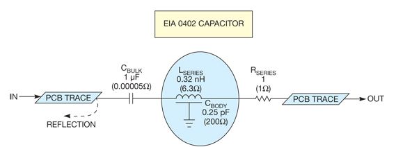
Figure 1 also highlights the key factors affecting performance at high frequencies. At 3.125 GHz, which corresponds to a 6.25 Gbps link operating in a 101010 pattern, the impedance of CBULK and RSERIES becomes minimal. However, LSERIES and CBODY play a critical role in determining the overall behavior of the circuit.
When analyzing a high-speed circuit, the first step is to evaluate the impedance of each component to determine which can be neglected. At 3.125 GHz, the impedance of the bulk capacitance and series resistance is almost insignificant, leaving the inductance and parasitic capacitance as the dominant factors. This makes the circuit behave like a portion of a trapezoidal model for distributed transmission lines.
When a rising edge reaches the input of the circuit, the response depends on the balance between the bulk capacitance and the series inductance. If the bulk capacitance is too large and the inductance is too small, the circuit acts as a negative pulse. Conversely, if the inductance is too high and the capacitance is too low, it behaves like a positive pulse. By carefully tuning the ratio of inductance and capacitance, the circuit can become nearly transparent, allowing signals to pass without distortion—this is the key to achieving excellent DC blocking performance.
One method to reduce the bulk capacitance is to introduce a small circular cutout in the ground plane beneath the capacitor. This allows some of the capacitance to be shunted to ground, slightly increasing the series inductance and raising the overall impedance. This technique helps to minimize unwanted reflections and improve signal integrity.
Some simulation engineers may recommend reducing the bulk capacitance until the resonant frequency formed by the bulk capacitance and series inductance aligns with 3.125 GHz. While this approach can be effective in narrowband applications, it may still leave residual parasitic capacitance, leading to reflections. To optimize performance, it’s often better to increase the bulk capacitance until its impedance becomes negligible, focusing instead on balancing the series inductance and bulk capacitance for near-ideal results.
Outdoor Grille LED Display,Weatherproof transparent LED screen,Outdoor see-through LED display,Glass Transparent LED Display,Outdoor transparent LED panel,Outdoor LED showcase display
Shenzhen Xinfei Century Technology Co., Ltd. , https://www.rgbdancing.com