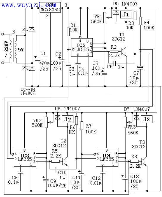
First, let's explore the working principle of the circuit.
This circuit is designed using three monolithic integrated circuits based on the LM555 timer IC. Each of these ICs functions as a monostable multivibrator, acting as a timing control unit. Together, they form a three-stage loop timing control system. When the power is first turned on, the reset pins (pin 4) of IC3 and IC4 are connected to automatic reset circuits with large time constants. These circuits consist of resistors R4 & C7 for IC3, and R7 & C11 for IC4. As a result, both IC3 and IC4 are initially in a reset state, causing their output pins (pin 3) to go low. This turns off transistors T2 and T3, which in turn releases relays J2 and J3.
Meanwhile, the reset pin (pin 4) of IC2 is directly connected to the positive supply voltage. At the moment of power-up, the capacitor C3 cannot change its voltage instantaneously, so the trigger pin (pin 2) of IC2 is activated, putting it into a temporary stable state. The output at pin 3 becomes high, which turns on transistor T1, allowing relay J1 to engage. This relay can be used to control an electrical appliance. At the same time, the power supply charges capacitor C5 through potentiometer VR1. Once the voltage across C5 reaches two-thirds of the supply voltage (approximately 4V), IC2 exits its temporary state, and the output at pin 3 goes low, turning off T1 and releasing relay J1. This cuts off the power to the appliance controlled by J1’s contacts.
The duration for which relay J1 remains engaged can be adjusted by changing the values of VR1 and C5. When IC2's output drops to a low level, a differentiating circuit composed of capacitor C6 and resistor R3 generates a negative spike at the trigger pin (pin 2) of IC3. This triggers IC3 into its transient state, causing its output (pin 3) to go high, which turns on transistor T2 and engages relay J2. The length of this timing period can be modified by adjusting VR2 and C9.
Similarly, when IC4’s timing ends, a differentiating circuit made up of capacitor C10 and resistor R6 produces a negative pulse at its trigger pin (pin 2). This activates IC4, leading to a high output at its pin 3, which turns on transistor T3 and engages relay J3. The timing duration for this stage can be fine-tuned by adjusting VR3 and C13. Finally, when the third stage completes its timing, the differentiating circuit involving C3 and R1 triggers the first stage again, completing the cyclic timing sequence.
PV pumping system is the use of solar modules to solar energy directly into electrical energy, drive motor driven pump device. Mainly divided into submersible pumps photovoltaic pumping and ground pumping photovoltaic pumping (suction stroke, different installation methods); PV pumping system: no fuel consumption, no power grid, almost no need for operation and maintenance, long service life, low average cost, especially for water and electricity shortage areas. Do not need batteries, solar modules directly driven by the pump work.
Solar Pump System,Solar Water Management System, Water Transfer Pump,Pumping Stations,DC Pump
Wuxi Sunket New Energy Technology Co.,Ltd , https://www.sunketsolar.com