The multi-channel synchronous digital phase modulation signal source is generally implemented by using a single chip microcomputer and a plurality of dedicated DDS chips. The technology is complex to implement and costly. A design method of multi-channel synchronous signal source based on FPGA is presented. The multi-channel synchronization signal based on single-chip FPGA is realized by VHDL language hardware programming, and the digital phase modulation is fast and accurate. The correctness of the design is verified by Quartus II synthesis and simulation. The design has the advantages of convenient phase modulation, high speed and low cost.
Introduction
The realization of multi-channel synchronous output of signal sources has important applications in many fields such as radar and communication. In order to achieve this function, most of the designs use multiple dedicated DDS chips to help achieve multi-signal synchronization output with the help of a single-chip microcomputer, as shown in Figure 1.
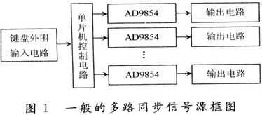
When the system works, according to the keyboard input, the MCU outputs the frequency control word and the phase control word and the waveform selection word, and controls the dedicated DDS chip AD9854 to generate a waveform of a specific frequency and phase, and outputs the required analog waveform after filtering and amplifying. For the output of the same frequency, phase-dependent multi-channel synchronization signal, the control data is input by the keyboard, and the MCU outputs the same frequency control word and different phase control word commands to each dedicated DDS chip to control the output frequency and phase of each dedicated DDS chip. Waveform. This achieves continuous adjustment and synchronization of frequency and phase as a whole.
The AD9854 is a DDS series of AD companies in the United States with good performance and wide frequency range. In such a design, the AD9854 chip of AD company is used, although the frequency is wide, the waveform is rich, and the characteristics of adjustment and frequency adjustment are easy. However, since the discrete dedicated DDS chip is used, it is difficult to implement the parameters of each chip. The exact same, the difference in parameters will cause the output signal frequency and phase to be different. Therefore, although each DDS chip uses the same frequency word, the frequency of each output signal is not completely the same. Similarly, due to inconsistent parameters, the phase between waveforms is difficult to accurately adjust to the position. More importantly, the cumulative effect of the difference in signal frequency may cause synchronization failure. In addition, dedicated DDS chips are expensive and costly to design.
Based on the above reasons, a design scheme of multi-channel synchronous signal source based on single-chip FPGA is presented. This scheme has the advantages of simple implementation, good synchronization, and low cost.
1 Design model of multi-channel synchronous signal source based on FPGA technology
The overall block diagram of the multi-channel sync signal source based on FPGA technology is shown in Figure 2.
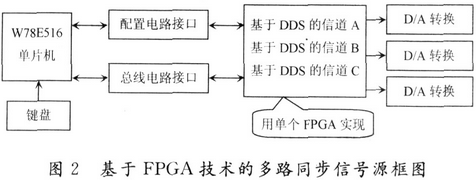
In this block diagram, taking three outputs as an example, in a FPGA chip, three DDs-based signal channels are implemented, and the functions of the traditional three dedicated DDS chips AD9854 are completed, and the digital output of the three-way waveform is realized. After the digital signal is output, D/A conversion is performed to realize analog output of the three signals. The three DDS channel frequencies are taken from the address value output by the same accumulator, and the table is checked. At the same time, the phase addition is also performed for the address of the same accumulator output, eliminating the error calculated by the discrete dedicated DDS chip. Since it is implemented in one chip, the parameters of each DDS channel are consistent, and the delay error caused by the external connection of the discrete dedicated DDS chip is also minimized. Therefore, through the above measures, the signal consistency can be greatly improved, and accurate phase continuous adjustment can be realized.
The single chip microcomputer and the bus configuration circuit realize the human machine interface through the keyboard. Through the 4 & TImes; 4 matrix keyboard, the frequency selection, initial phase selection and other data can be input into the MCU and sent to the FPGA after being processed by the MCU to realize the DDS adjustment.
The FPGA is the core component for completing DDS multi-signal generation, and completes the generation of DDS multi-channel synchronization signals.
2 FPGA core design of multi-channel sync signal output based on DDS technology
2.1 General DDS works
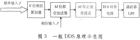
DDS (Direct Digital Synthesizer) is a frequency synthesis technique that directly synthesizes the required waveforms from the phase concept. A DDS signal generator is composed of: phase accumulator, waveform number ROM table, D/A converter and analog low-pass filter LPF. The block diagram is shown in Figure 3. The core of DDS technology is the phase accumulator. The phase accumulator generates the address value of the read data under the control of the stable clock signal. Then, by looking up the table, the address value is converted into the digital amplitude sequence of the signal waveform, and then the digital/modulo The converter (D/A) converts the digital sequence representing the amplitude of the waveform into an analog voltage, and finally smoothes the staircase waveform of the D/A output to the desired continuous waveform via a low-pass filter. The phase accumulator is accumulated by the step F under the control of the clock Fc, and the output value is added to the phase control word P to form an address value of the look-up table, and the waveform ROM is addressed. The output value of the waveform ROM is the amplitude value, which is transformed into a staircase waveform after D/A conversion, and finally smoothed into a desired waveform by low-pass filtering. The waveform of the composite signal depends on the amplitude sequence in the ROM table. By modifying the data, an arbitrary waveform can be generated. If multiple waveforms are to be generated, only a plurality of waveform data required are stored in the waveform ROM table. The schematic diagram of the general DDS is shown in Figure 3.
Mainly used for Solar power storage system, home solar system, this kind of battery has more than 2500 cycle life.
LFPS series lithium battery using LiFePO4 battery cells with more advantages as following:
â—† Longer life compare to lead acid battery
â—† Up to 60% weight saving
â—† 100% usable capacity
â—† More energy with 1/3 smaller size
â—† Less than 3% self discharging
â—† Built in safety protection
â—† Zero maintenance
â—† Easy installation
â—† Eco-friendly
â—† Quality guaranteed
LiFePO4 Solar Energy Storage Batteries
Solar Power Battery,Portable Solar Power Battery,Lithium Solar Power Batteries,Solar Power Deep Cycle Battery
Starlight Power Industrial Company Limited , https://www.starlite-power.com