Designing an electronic circuit that introduces a power delay after the switch is turned on can be very useful in many applications. This type of circuit allows the system to remain off for a set period before turning on again, which can be particularly helpful when you want to avoid sudden power surges or ensure proper stabilization before activating certain components. Instead of using a relay, a transistor-based solution can also be used to achieve a similar delay effect for DC voltage turn-on.
In some cases, it's necessary to delay the power-up of a device after the switch is activated. For instance, in audio amplifiers, it’s important to wait until the amplifier stabilizes before connecting the speaker to prevent damage or unwanted noise. Similarly, in other devices with output stages, delaying the activation ensures that all internal circuits are fully powered and ready before any external load is connected.
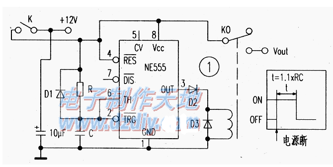
Figure 1 shows a basic delay circuit using a 555 timer IC as the time base. This circuit delays the activation of a relay for a specific period after the power switch is turned on. The delay time is determined by the values of resistor R and capacitor C. When R is 100kΩ and C is 10μF, the delay is approximately 1.1 seconds. This setup is ideal for applications where a relay is acceptable and more robust switching is required.
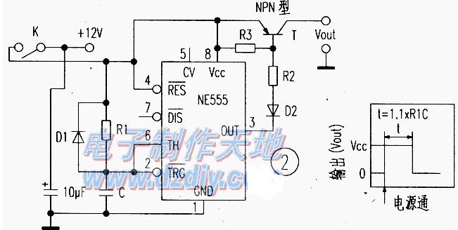
If a relay is not preferred, a transistor-based circuit can serve the same purpose. Figure 2 illustrates such a design. In this configuration, a PNP transistor is used to control the DC voltage output. When the switch is activated, the circuit triggers a monostable mode in the 555 timer, which keeps the output high for a defined period. During this time, the transistor remains off, preventing the output from being connected to the power supply. Once the delay has passed, the transistor turns on, allowing the DC voltage to reach the load.
Both circuits operate similarly when the manual switch K is connected to the +12V power supply. The 555 timer starts its timing cycle, and the output pin (pin 3) goes high. In the first circuit, this activates the relay, which then connects the load to the power supply. In the second circuit, the high signal turns on the PNP transistor, allowing the output voltage to be delivered to the connected device.
These delay circuits are simple yet effective solutions for managing power sequencing in various electronic systems. Whether using a relay or a transistor, the key is to choose the right components based on the application requirements, such as current handling, response time, and reliability. Understanding how these circuits work can help engineers design more stable and efficient power control systems.
Ring Common Mode Inductor,UU Common Mode Inductor,Vertical Plug-in Common Mode Inductor,Power Line Common Mode Choke
Xuzhou Jiuli Electronics Co., Ltd , https://www.xzjiulielectronic.com