In electronic production and design, inductors with different parameters are often used. The inductance of these coils is not as easy to measure as resistors. Some digital multimeters have inductive measurement, but the measurement range is limited. The circuit measures the inductance value by the resonance method. The lower limit of measurement can reach 10nH, and the measurement range is wide. It can meet the measurement of inductance under normal conditions, the circuit structure is simple, the work is reliable and stable, and it is suitable for enthusiasts.
First, the circuit working principle The circuit principle is shown in Figure 1 (a).
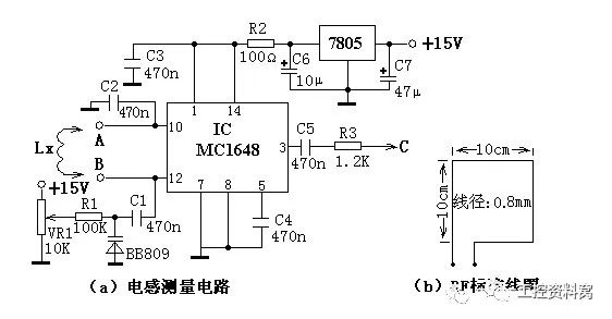
Figure 1 Simple inductance measuring device circuit diagram
The core device of the circuit is the integrated voltage-controlled oscillator chip MC1648, which uses its voltage-controlled characteristic to generate a frequency signal at the output 3 pin, which can indirectly measure the LX value of the inductor to be tested, and the measurement accuracy is extremely high.
BB809 is a varactor. In the figure, potentiometer VR1 divides +15V. Adjusting the potentiometer can obtain different voltage output. This voltage can be added to varactor BB809 through R1 to obtain different capacitance. When measuring the measured inductance LX, just connect LX to the two points A and B in the figure, then adjust the potentiometer VR1 to make the circuit resonate. In the MC1648, the 3rd pin will output the oscillation signal of a certain frequency, and the frequency meter will measure the C point. The frequency value can be calculated by calculating the LX value.
Circuit resonance frequency: f0 = 1/2p
So LX = 1/4p2 f02C
In the formula, the resonant frequency f0 is the output frequency of the 3 pin of the MC1648, and C is the capacitance value of the varactor diode set by the potentiometer VR1. It can be seen that the value of LX needs to know the value of C first. To do this, it is necessary to calibrate the corresponding value of the potentiometer VR1 scale and the varactor.
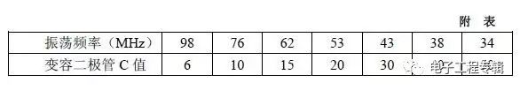
In order to calibrate the capacitance between the varactor and the potentiometer, we have to make a standard square RF (radio frequency) inductor L0. As shown in Figure 6-7(b), the standard coil inductance is 0.44mH. During calibration, connect the RF coil L0 to both ends of A and B of Figure (a), adjust the potentiometer VR1 to different scale positions, measure the corresponding measured value at point C, and calculate the change according to the above resonance formula. The capacitance of the diode on different scales of the potentiometer VR1 dial. The attached table gives the corresponding relationship between the measured samples.
Second, the component selection
The integrated circuit IC can be selected from Motorola's VCO (Voltage Controlled Oscillator) chip. VR1 selects multi-turn high-precision potentiometers. Other components can be selected as shown in the circuit diagram.
Third, the production and debugging method production, you need to make a dial on the multi-turn potentiometer shaft, and bring the pointer. The RF standard coil is self-made according to the dimensions given in Figure (b). The circuit can be installed normally, and the potentiometer VR1 can adjust the corresponding relationship between multiple points of sliding and varactor diodes to ensure convenient measurement. This measurement method is an indirect measurement, but the measurement range is wide and the measurement is accurate, so it is desirable for electronic enthusiasts and laboratories to detect inductance. The device can be turned into a signal generator with an adjustable frequency if the inductor is fixed. Circuit 2 Three-digit display capacitance test table The majority of electronic enthusiasts have this experience. Although the medium and high-end digital multimeter has a capacitance test gear, the measurement range is generally only 1pF~20ïF, which often cannot meet the needs of users. , causing inconvenience to capacitance measurement. The three-digit display capacitance test table introduced by this circuit adopts four integrated circuits. The circuit is simple, easy to manufacture, digital display is intuitive, and the precision is high. The measurement range can reach 1nF~104ïF. Especially suitable for lovers and electrical maintenance personnel to make and use.
First, the circuit working principle The circuit principle is shown as in Fig. 2.
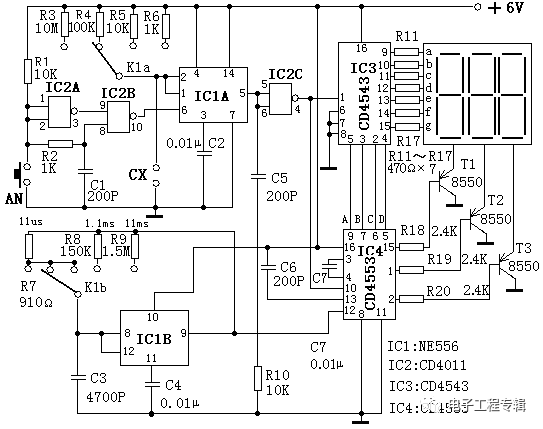
Figure 2 Three-digit display capacitance test chart circuit diagram
The capacitance meter circuit is composed of a reference pulse generator, a capacitance capacity time converter to be tested, a gate controller, a decoder, and a display.
The capacitance capacity time converter to be tested converts the capacity of the measured capacitance into a one-shot time td proportional to its capacity value. The reference pulse generator produces a standard cycle count pulse. The turn-on time of the gate controller is the one-shot time td. During the td time, the cycle count pulse is sent to the back counter through the gate, and the decoder drives the display to display the value. The period T of the counting pulse multiplied by the count value N displayed by the display is the one-shot time td. Since td is proportional to the capacity of the capacitor to be measured, the capacity of the capacitor to be measured is also known.
In Figure 2, the integrated circuit IC1B resistors R7~R9 and capacitor C3 form the reference pulse generator (essentially an unstable multivibrator), and the output pulse signal period T is related to R7~R9 and C3, fixed in C3. In the case of different selections of R7, R8, and R9 by the range switch K1b, three pulse signals having periods of 11 ï, 1.1 ms, and 11 ms can be obtained.
IC1A, IC2, R1~R6, buttons AN and C1 form a time-constant capacitor (substantially a one-shot circuit) to be tested. Pressing AN once, IC10B's 10 pin produces a negative narrow pulse trigger IC1A, and its 5 pin outputs a single high level signal. R3~R6 and the capacitor CX to be tested are single-stability components, and the one-shot time td=1.1 (R3~R6)CX.
IC4, IC2C, C5, C6, R10 form the gate controller and counter. IC4 is CD4553. Its 12-pin is the count pulse input terminal, and the 10-pin is the count enable terminal. CD4553 performs counting at low potential, and 13-pin is count clear. End, the rising edge is valid. When the AN is pressed, the 13 pin of IC4 gets a rising pulse, the counter is cleared, and the 4 pin of IC2C outputs a one-shot low level signal to the 10 pin of IC4, so IC4 counts the reference input from its 12-pin. The pulse is counted. When the one-shot time is over, IC4's 10 pin becomes high level, IC4 stops counting, and finally IC4 passes the counting result of one digit, ten digits, hundred digits by its 9-pin, 7-pin, 6 by time-sharing transmission. The foot and the 5 foot loop output the corresponding BCD code.
IC3 constitutes the decoder driver, which translates the BCD code sent from IC4 into a decimal digital pen segment code, and directly drives the seven-segment digital tube after R11~R17 current limit. The 15th, 1st, and 2nd pins of the integrated circuit CD4553 are digital selection outputs. The pulses are sent to the bases of the transistors T1~T3 through R18~R20 to make them turn on. The two parts are matched to complete the three-digit decimal. Digital Display.
The role of C7 is to generate a rising pulse on R10 when the power is turned on, and the counter is automatically cleared.
Second, in the component selection circuit, IC1 selects NE556; IC2 selects CD4001; IC3 selects CD4543; IC4 selects CD4553. The seven-segment digital tube can be used with a three-word common cathode digital tube. 850 (or other PNP type triode) is used for T1~T3. C1 should not be larger than 0.01ïF, and C3 should use small metallization capacitors. R3~R9 use 1/8W metal film resistor. There are no special requirements for other components, and you can select them according to the circuit labeling.
Third, the production and debugging method After the entire circuit is installed, it can be installed in a plastic box, and the digital tube and the range switch are mounted on the panel. In the production and debugging, the key is to call up the three standard pulse signals of 11ïs, 1.1ms and 11ms. When debugging, you need to adjust the resistance of three resistors, such as R7, R8 and R9, by means of an oscilloscope. These three pulse signals can be conveniently obtained. The resistance values ​​of R7, R8 and R9 in the circuit are experimental data for reference only. The rest of the circuit does not need to be debugged. As long as the good device is selected, the installation is correct, and the corresponding override is marked at the range switch, a practical, accurate and reliable digital capacitance meter can be obtained.
Fourth, the method of use
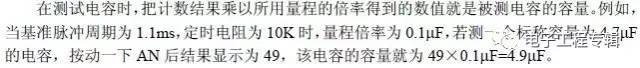
It should be noted that when using the 1pF~999pF range, the measurement result minus the distributed capacitance value is the accurate value of the measured capacitance due to the influence of the distributed capacitance. The range distribution capacitance value of the capacitance meter can be measured in this way, and the range is set in the range of 1pF to 999pF. When the measured capacitance is not connected, the AN button is pressed, and the measured result is the distributed capacitance value of the block. The value is generally about 10 pF after experimentation. The schedule lists the compositional relationships of the various ranges. Schedule

Circuit 3 Mains voltage bidirectional over-limit alarm protector The alarm protector can perform sound and light alarm when the mains voltage is higher or lower than the specified value, and automatically cut off the electrical power supply to protect the electrical appliance from damage. The device is small in size, full in function, simple in manufacture and practical.
First, the circuit working principle The circuit principle is shown in Figure 3.
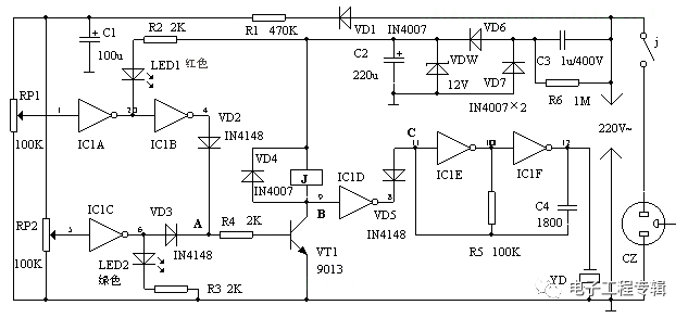
Figure 3 Mains voltage bidirectional over-limit alarm protector circuit diagram Mains voltage one route C3 step-down, DW regulator, VD6, VD7, C2 rectification and filtering output 12V stable DC voltage supply circuit. Another route VD1 rectification, R1 step-down, C1 filtering, generating a voltage of about 10.5V on RP1, RP2 to detect the mains voltage change input signal. The gate IC1A and IC1B form an overvoltage detection circuit, IC1C is undervoltage detection, IC1D is a switch, IC1E, IC1F and piezoelectric ceramic piece YD constitute an audio pulse oscillator. The triode VT and the relay J constitute a protection action circuit. The red LED1 is used as the mains overvoltage indication, and the green tube LED2 is used as the mains undervoltage indication.
When the mains is normal, non-IC1A outputs a high level, IC1B, IC1C output low level, LED1, LED2 are off and no light, VT is off, J does not operate, the appliance is normally powered, B point is high, F4 output Low level, VD5 is on, C is low, the audio pulse oscillator is stopped, and YD is not sounding. When the mains is overvoltage or undervoltage, IC1B and IC1C have one output high level, which makes point A become high potential, VT saturation turns on, J energizes and pulls, disconnects the electrical power supply, and B point becomes Low potential, IC1D output high level, VD5 cut-off, reverse resistance is large, equivalent to open circuit, audio pulse oscillator starts, YD sounds alarm, and the corresponding LED emits light.
Second, the choice of components Integrated chip IC can choose CD74HC04 six inverter, diode VD1 ~ VD6 select IN4007, capacitor C1 ~ C6 select aluminum electrolytic capacitor, withstand voltage 400V, regulator tube selects 12V voltage regulator, relay J selects general 6V DC relay can be used, the resistor uses ordinary 1/8 or 1/4W carbon film resistor, the size can be as shown.
3. When debugging and debugging , use a voltage regulator to supply power, adjust the voltage to normal value (220V), use an incandescent lamp as load, make LED1 and LED2 go out, incandescent light, then adjust the regulator to Limit value or lower limit value, adjust RP1 or RP2 to make LED1 or LED2 just light, and the incandescent light is off, that is, the debugging is successful. All components can be installed in a small plastic box, two holes are fixed on the lid to fix the LED, a larger round hole is used to fix the piezoelectric ceramic piece, and a suitable cap is used to help the piezoelectric piece. The sound chamber makes it sound louder. Circuit 4 Infrared detection burglar alarm This alarm can detect the infrared rays emitted by the human body. When a person enters the monitoring area of ​​the alarm, it can sound an alarm. It is suitable for burglar alarms in important places such as home, office, warehouse, and laboratory.
First, the circuit working principle The circuit principle is shown in Figure 4. The device is composed of an infrared sensor, a signal amplifying circuit, a voltage comparator, a delay circuit and an audible alarm circuit. When the infrared detecting sensor IC1 detects the infrared signal radiated from the front human body, the weak electric signal is output from the 2 pin of the IC1, and is amplified by the first-stage amplifying circuit through the triode VT1, and then input to the operational amplifier IC2 through C2 for high gain. Low noise amplification, at this time the signal output by the IC21 pin is strong enough. IC3 is used as the voltage comparator. Its 5th pin provides the reference voltage from R10 and VD1. When the signal voltage output from IC21 pin reaches the 6th pin of IC3, the voltages of the two input terminals are compared. At this time, the 7th pin of IC3 is from the original The high level goes low. IC4 is the alarm delay circuit, and R14 and C6 form a delay circuit, which takes about 1 minute. When IC3's 7 pin goes low, C6 discharges through VD2. At this time, IC4's pin 2 goes low. It compares with IC4's 3-pin reference voltage. When it is lower than its reference voltage, IC4's The 1 pin becomes high level, VT2 turns on, and the alarm BL energizes to sound an alarm. After the infrared signal of the human body disappears,
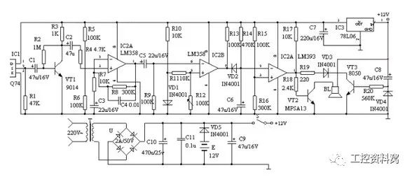
Figure 4 Infrared detection burglar alarm circuit diagram IC3's 7 feet return to high level output, VD2 is cut off at this time. Since the voltage across C6 cannot be abrupt, it is slowly charged to C6 through R14. When the voltage across C6 is higher than its reference voltage, the 1 pin of IC4 becomes low level for about 1 minute, that is, the alarm is continued for 1 minute. . The power-on delay circuit consists of VT3, R20 and C8, and the time is also about 1 minute. Its setting is mainly to prevent the user from immediately alarming after starting the machine, so that the user has enough time to leave the monitoring site and prevent the power failure after the power failure. A false positive occurred while calling. The device is powered by 9-12V DC power supply, step-down by T, full-bridge U rectification, C10 filtering, detection circuit is powered by IC5 78L06, AC and DC, automatic and uninterrupted conversion.
Second, the component selection IC1 uses imported device Q74, the wavelength is 9-10um. IC2 uses the op amp LM358 with high gain and low power consumption. IC3 and IC4 are dual voltage comparators LM393, low power consumption and low offset voltage. In C2 and C5, it is necessary to use a tantalum capacitor with a small leakage electrode, otherwise the debugging will be affected. R12 is a key component for adjusting sensitivity, and a linear high-precision sealing type should be used. Other components can be selected as shown in the circuit diagram.
Third, the production and debugging methods are made, the Fresnel lens is installed in front of the end of the IC1 sensor, because the human body's active frequency range is 0.1-10Hz, the Fresnel lens needs to double the human activity frequency. Installation is correct, connect the power supply for debugging, let a person walk around 7-10m in front of the detector, adjust R12 in the circuit, so that the alarm can be alarmed. As long as the components are of good quality and the welding is correct, the other parts can work normally without debugging. The static working current of the machine is about 10 mA. After the power is turned on for about 1 minute, it enters the waiting state. As soon as someone enters the monitoring area, it will alarm, and the person will stop the alarm about 1 minute after leaving. If the sounder is changed to a relay to drive other devices, it is used for other control. Circuit 5 Non-Smoking Alerts The smoking ban warnings described in this example can be used in homes or in places where smoking is not appropriate (eg hospitals, conference rooms, etc.). When someone smokes, the no-smoking warning device will issue a "Please do not smoke!" language warning to remind the smoker to consciously stop smoking.
First, the circuit working principle The circuit principle is shown as in Fig. 5. The smoke-free warning circuit is composed of a smoke detector, a monostable trigger, a language generator and a power amplifying circuit, and the smoke detector is composed of a potentiometer RP1, a resistor R1 and a gas sensor. The monoflop is composed of a time base integrated circuit IC1, a resistor R2, a capacitor C1, and a potentiometer RP2. The speech generator circuit is composed of a voice integrated circuit IC2, a resistor R3-R5, a capacitor C2, and a Zener diode VS. The audio power amplifying circuit is composed of a transistor V, a boosting power amplifier module IC3, resistors R6 and R7, capacitors C3 and C4, and a speaker BL.
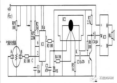
Fig. 5 Circuit diagram of the non-smoking warning device When the smoke sensor detects smoke at the end, the resistance of the two ends of A and B is large, the 2 pin of IC1 is high level (higher than 2Vcc/3), and the output of 3 pin is low. Ping, the voice generator circuit and the audio power amplifier circuit do not work, and the BL does not sound.
When someone smokes and the gas sensor detects smoke, the resistance values ​​of the two ends of A and B become smaller, so that the voltage of pin 2 of IC1 drops. When the voltage of the foot drops to VCC/3, the one-shot trigger Flip, IC1's 3 pin changes from low level to high level. After high level R3 current limit, C2 filtering and VS voltage regulation, 4, 2V DC voltage is generated, which is supplied to voice integrated circuit IC2 and crystal arm. After IC2 is powered on, it outputs a voice electric signal. After the electric signal is amplified by V and IC3, it pushes the BL to issue a "Please do not smoke!" voice warning sound.
Second, the component selection Rl-R7 selects 1/4W carbon membrane resistor or metal membrane resistor. Small linear potentiometers or variable resistors are available for RP1 and RP2. C1, C2 and C4 are all selected from aluminum electrolytic capacitors with a withstand voltage of l6V; C3 is a monolithic capacitor. VS selects 1/2W, 4·2V silicon Zener diode. V selects S9013 or C8050 type silicon NPN transistor for use. IC1 selects NE555 type time base integrated circuit; IC2 selects voice integrated circuit with "Please do not smoke!" voice information; lC3 selects WVH68 type boost power amplifier thick mode integrated circuit. BL uses 8Ω, 1-3W electric speakers. The gas sensor is a MQK-2 type sensor.
Third, the production and commissioning of the anti-smoking warning device, can be used as a smoke alarm to detect fire or as a detection of harmful gases, flammable gases. Adjusting the resistance of RP1 can change the heating current of the gas sensor (generally about 13OmA). Adjusting the resistance of RP2 can change the sensitivity of the monostable trigger circuit action. 6 circuit 555 uses a simple temperature controller circuit according to the circuit substrate is to use an automatic temperature controller 555 IC and a few external components thereof. Because the voltages at various points in the circuit are from the same DC power supply, there is no need for a regulated power supply with good performance, and the capacitor step-down method can work reliably. Circuit components are low in price, small in size, and easy to make in amateur conditions. The temperature automatic controller made by this circuit can be used for industrial heating and electric heating control of households with good effect.
First, the circuit working principle The circuit principle is shown in Figure 6.
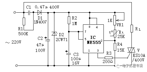
Figure 6. Simple temperature controller circuit diagram with 555 time base circuit. When the temperature is low, the negative temperature coefficient thermistor Rt has a large resistance value. The 555 time base integrated circuit (IC) has 2 pin potentials lower than the Ec voltage. /3 (about 4V), the IC 3 pin outputs a high level, triggers the bidirectional thyristor V to conduct, and turns on the electric heater RL for heating, thereby starting the timing cycle. When the temperature of the thermistor Rt placed at the temperature measuring point is higher than the set value and the timing cycle has not been completed, the heater RL is cut off after the end of the timing period. When the thermistor Rt temperature drops below the set value, the triac V is turned on again, and the electric heater RL is turned on for heating. This will achieve the purpose of automatic temperature control.
Second, the component selection circuit, the thermistor Rt can use the negative temperature coefficient of the MF12 type or MF53 type, you can also choose different resistance values ​​and other models of negative temperature coefficient thermistor, as long as the temperature conditions required The relationship of Rt+VR1=2R4() can be satisfied. The larger the potentiometer VR1 can achieve a larger adjustment range, but the sensitivity will decrease. The triac V can also be selected according to the magnitude of the load current. There are no special requirements for other components, and parameters are selected according to the circuit diagram.
Third, the production and debugging methods The entire circuit can be installed on a circuit board, generally do not need to debug, the time interval is 1.1R2 × C3, should be selected smaller than the heating system's thermal time constant, but it can not be too small, otherwise it will Excessive RF interference is caused by the rapid turn-on or turn-off of the triac V. After installation and commissioning, it can be loaded into a small plastic box and the thermistor Rt can be taken out to the temperature measurement point. Circuit 7 uses an automatic temperature controller of the 555 time base circuit. This circuit can control the state of operation of the powered device by the change of temperature.
First, the circuit working principle The circuit principle is shown in Figure 7.
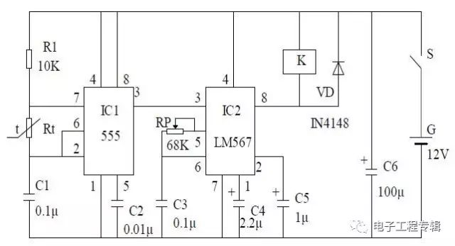
Figure 7: Automatic temperature controller circuit diagram using 555 time base circuit IC1 555 integrated circuit is connected to self-excited multivibrator, Rt is thermistor, when the ambient temperature changes, by resistor R1, thermistor Rt, The oscillation frequency composed of the capacitor C1 will change. The frequency change is sent to the 3 pin of the frequency decoding integrated circuit IC2 LM567 through the 3 pin of the integrated circuit IC1 555. When the input frequency falls exactly at the center frequency of the IC2 integrated circuit, 8 feet Output a low level, so that the relay K is turned on, the contacts are attracted, thereby controlling the on and off of the device to form a temperature control circuit.
Second, the choice of components IC1 selects NE555, μA555, SL555 and other time base integrated circuits; IC2 selects LM567 frequency decoding integrated circuit; VD selects IN4148 silicon switch diode; R1 selects RTX-1/4W type carbon film resistor. C1, C2, C3 select CT1 ceramic capacitor; C4, C5 select CD11-25V type electrolytic capacitor; K selects JZC-22F small medium power electromagnetic relay with working voltage 9V; Rt can use 51KΩ negative temperature coefficient thermal at normal temperature Resistor; RP can be WSW type organic solid fine-tuning variable resistor.
Third, the production and debugging methods In the production process, as long as the circuit is correct, this circuit is very easy to implement, if the component performance is good, you do not need to debug after installation. Circuit 8 adopts the CD4011 over-temperature monitoring automatic control circuit. The circuit has a simple structure and is easy to manufacture. A NAND gate and a thermistor constitute a measurement and control circuit and a siren sound circuit, and a relay is used as an execution circuit.
First, the circuit working principle The circuit principle is shown in Figure 8.

Figure 8 Using the CD4011 over-temperature monitoring automatic control circuit diagram Temperature measuring resistor RT is connected to the input terminal of the control gate D1, it and the resistors R1, R2 and RP through the RP partial pressure adjustment, so that the input level of the gate D1 is high , make D1 output low.
When in use, the thermistor RT is placed on the controlled device. When the temperature of the controlled device exceeds the maximum set temperature, the voltage of the D1 input becomes low due to the small voltage of the RT. After D1 is inverted to a high level, the high level is applied to the control terminal 8 of the multivibrator on the one hand, so that the multivibrator starts to oscillate, and after being amplified by the amplification tube, the siren sound is emitted by the speaker, and is also added to The base of VT1 is turned on, the relay is sucked, and the working power of the controlled device is disconnected through the normally closed contact of the relay; on the other hand, after the D2 is inverted to the low level, the LED of the LED is formed through the light. , LED lighting instructions.
Second, the choice of components IC1 selects CD4011; VD selects IN4001; VS is regulated voltage regulator 10V; VT1 selects 9013, VT2 selects V40AT; capacitor C is 2000P ceramic chip capacitor; relay is 4099 relay; RP selects 470K Ordinary adjustable potentiometer; resistors use 1/8 or 1/4W metal film resistors, BL selects 8Ω, 0.5W electric speakers.
Third, the production and debugging method The temperature measuring resistor RT is placed at the highest limit temperature, adjust the RP, so that the monitoring circuit emits a siren and the relay sucks and works, then the RT is cooled, the siren should stop. Otherwise, the RP should be adjusted repeatedly until it meets the requirements. Circuit 9 Digital Thermometer Circuit This circuit is a thermometer made by applying the integrated temperature sensor of AD590. It has the characteristics of simple structure, reliable use and high precision.
First, the circuit working principle The circuit principle is shown in Figure 9.
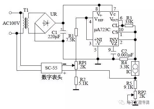
Figure 9 Digital thermometer circuit diagram 100V AC voltage through the transformer T1, rectifier bridge stack UR and capacitor C1, to obtain a DC voltage, and then through the adjustable regulator circuit μA723C to provide a stable operating voltage for the temperature sensor AD590. The AD590 temperature sensor is a new type of current output type temperature sensor consisting of multiple transistors and resistors with the same parameters. When a specific DC operating voltage is applied to both ends of the sensor, if the temperature of the temperature sensor is 1 degree Celsius, the output current of the sensor changes by 1 μA. The changing current of the sensor is converted into a voltage signal through the resistor R5 and the variable resistor RP2, and output to the digital meter, and the temperature change is displayed by a digital meter.
Second, the component selection integrated circuit IC selects the AD590 type temperature sensor. There are no special requirements for other components of this circuit, and can be selected according to the parameters given in the circuit diagram.
Third, the production and debugging methods can change the sensitivity of the output by changing the value of the resistor R5 and the variable resistor RP2. Circuit 10 Tropical fish tank water temperature automatic controller Tropical fish tank water temperature automatic controller uses a negative temperature coefficient thermistor as a temperature probe to automatically heat the fish tank through heating gas. The transient time of this circuit is small, which is beneficial to temperature control accuracy and is applicable to fish tanks of various sizes.
First, the circuit works The circuit diagram shown in Figure 10. After the diodes VD2~VD5 are rectified and the capacitor C2 is filtered, a voltage of about 12V is supplied to the control portion of the circuit. The 555 time base circuit is connected to a monostable flip-flop with a transient state of 11 s. Set the control temperature to 25oC, by adjusting the potentiometer RP so that RP + Rt = 2R1, Rt is a thermistor with a negative temperature coefficient. When the temperature is lower than 25oC, the resistance of Rt rises, and the 2 pin of the 555 time base circuit is low level, then the 3 pin changes from the low level output to the high level output, the relay K is turned on, and the contacts are attracted. The heating tube starts to heat until the temperature returns to 25oC, the resistance of Rt becomes smaller, the 2 pin of the 555 time base circuit is at a high level, the 3 pin outputs a low level, the relay K loses power, the contact is disconnected, and the heating stops.
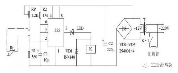
Figure 1 0 Tropical fish tank water temperature automatic controller circuit diagram 2, component selection IC selects NE555, μA555, SL555 and other time base integrated circuits; VD1 selects IN4148 silicon switch diode; LED selects ordinary light-emitting diode; VD2~VD5 selects IN4001 type silicon rectifier Diode; Rt selects 470Ω MF51 type negative temperature coefficient thermistor at room temperature; RP selects WSW organic solid trimmer potentiometer for RW; RXT-1/8W type carbon film resistor for R1 and R2; CD11-16V type for C1 and C3 Electrolytic capacitor; C2 selects CT1 ceramic
(1)")
Multi-function, multi-device charging solution - With a large 20,000 mAh built-in battery, the mophie Powerstation XXL High Capacity mobile Power supply charges your phone super fast and can fully charge your phone up to 4.6 times. Charge three devices simultaneously
Charge Your Devices Fast - With 18W USB-C power output, charge your phone the fastest and get up to 50% battery power in just 30 minutes. The USB-C port can be used to charge the power station itself during recording hours.
Compatible with various gadgets - In addition to the USB-CpD port, the Portable Portable Power Supply also comes with 2 USB-A ports for charging smartphones, tablets, and other USB devices. The package includes a charging cable (USB-A to USB-C).Functional and stylish - With a classic fabric finish that prevents scuffs and scratches, this mobile power supply is your perfect travel companion. Easily fit in your bag, so you can carry it to work or on adventures without a separate charger
Its main components include: a battery for electrical energy storage, a circuit (DC-DC converter) to stabilize the output voltage, and most mobile power supplies come with a charger for charging as a built-in battery.
100W Power Bank,power bank price,portable phone charger,power bank 30000mah
suzhou whaylan new energy technology co., ltd , https://www.xinlingvideo.com