1. Introduction of network transformer
The network transformer is also called "data mercury" and can also be called a network isolation transformer. It plays a role in a network interface, there are two main, one is to transmit data, it sends the differential signal from the PHY with a differential-mode coupled coil coupling filter to enhance the signal, and coupled to different levels through the electromagnetic field conversion The other end of the connection network cable; the first is to isolate different levels between different network devices connected by the network cable to prevent different voltages from transmitting the damaged device through the network cable. In addition, data mercury can also provide some lightning protection to the equipment. It is mainly used in network switches, routers, network cards, and hubs, and functions as signal coupling, high-voltage isolation, impedance matching, and electromagnetic interference suppression.
Network transformer design topology for switch and network card:
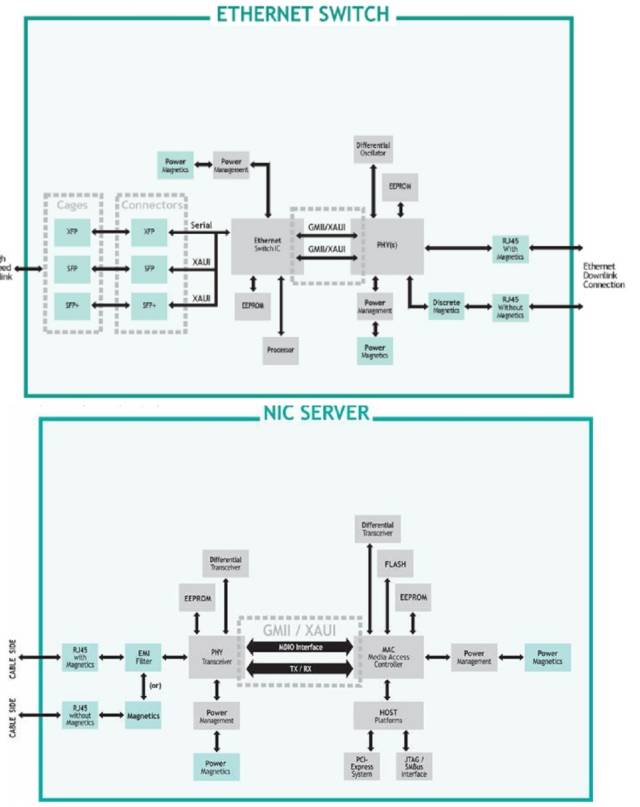
Ethernet equipment uses a transformer between the transceiver and the network cable, which includes a center-tapped transformer, an autotransformer, and a common-mode inductor. The latest Ethernet devices provide 48V power through transformers and use integrated connectors for more and more applications. The characteristics of these devices are critical to the suppression of EMI.
2, network transformer classification
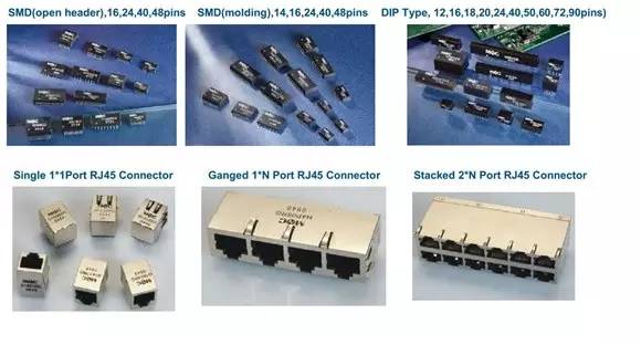
Products can be divided into two types according to the structure type: a. Discrete LAN Magnetics Module; b. RJ45 Connector with Integrated Magnetics (ICMs).
Products can be classified into two types based on customer welding types: a. Surface Mount Type (SMT), and Surface Type Type (TH), Through-Hole Type (TH).
Products based on transmission rate, can be classified into four categories: a. 10Base-T, b. 10/100Base-T, c. 1000 Base-T, d. 10G Base-T.
(Base-T: Baseband, twisted pair. In short, Base-T is a local area network (LAN) standard that operates at a bps rate. It is often referred to as Fast Ethernet and uses UTP (unshielded dual). Stranded copper cables. Fast Ethernet has three basic implementations: Base-FX, Base-T, and 1Base-T4. Each specification is the same except for the interface circuit, which determines where they are used. This type of cable uses the 4B/5B Manchester Encoding mechanism for clock/data recovery (CDR) functions.)
3, the working principle of the network transformer:
3.1 Internal Structure
1. Common mode choke (CMC: Common mode Choke)
Common mode chokes, also known as common-mode choke inductors, are symmetrical windings of opposite coils with the same number of turns on a closed magnetic ring. The ideal common mode choke coil has an inhibitory effect on the common-mode interference between L (or N) and E, while there is no inductance suppression effect on the differential mode interference existing between L and N. However, the incomplete symmetry of the actual coil winding will lead to the leakage inductance of the differential mode. When the signal current or the supply current flows in opposite directions in the two windings, the generated magnetic flux cancel each other, and the choke coil exhibits low impedance. Common-mode noise currents (including disturbance currents caused by ground loops, also referred to as longitudinal currents) flow in the same direction across the two windings. The resulting magnetic fluxes add in the same direction, and the choke coils exhibit high impedance, which suppresses common The role of mode noise. A common-mode inductor is essentially a bi-directional filter: on the one hand, common-mode electromagnetic interference on the signal line must be filtered out, and on the other hand, it must prevent itself from sending out electromagnetic interference and avoid affecting the normal operation of other electronic devices under the same electromagnetic environment. .
Common-mode chokes can transmit differential-mode signals, and differential-mode signals with low DC and very low frequencies can all pass through. However, common-mode chokes can exhibit high resistance to high-frequency common-mode noise. Therefore, they can be used to suppress common-mode current disturbances.

Common-mode choke coils are an important part of switching power supplies, inverters, and UPS power supplies. Its working principle: When the working current flows through two opposite coils, two magnetic fields H1 and H2 cancel each other out. At this time, the operating current is mainly affected by the ohmic resistance of the coil and negligible damping of the small leakage inductance at the working frequency. . If there are interference signals flowing through the coil, the coil will show a high impedance, which will produce a strong damping effect and achieve the purpose of attenuating the interference signal.
CMC suppresses common-mode signals:
As the name implies, a common mode choke coil is a component for suppressing a common mode noise signal (useless signal, interference signal). It forms a high impedance to a common mode noise signal and basically has no effect on a differential mode signal (useful signal). . It is the main component to suppress EMI interference. Its working principle is as follows:
The common-mode signal refers to the input of the same polarity signal at both inputs. Common-mode signals will cause electromagnetic interference. Electromagnetic interference is divided into radiation interference and conduction interference (into the power line). Differential signal conversion during signal transmission asymmetry and impedance mismatch will generate common-mode signals for digital terminal equipment.
CMC has no effect on differential mode signals:

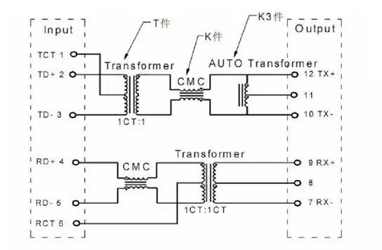
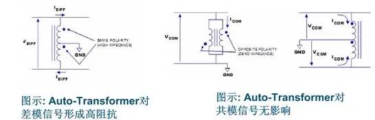
2. Center Tapped Auto-Transformer
The self-coupling transformer forms a high impedance to the differential mode signal, and basically has no influence on the common mode signal. According to the above connection mode, the signal can be transmitted effectively, and then the electromagnetic interference is further reduced and suppressed.
3, choke coil working principle and insertion loss characteristics (or impedance characteristics):
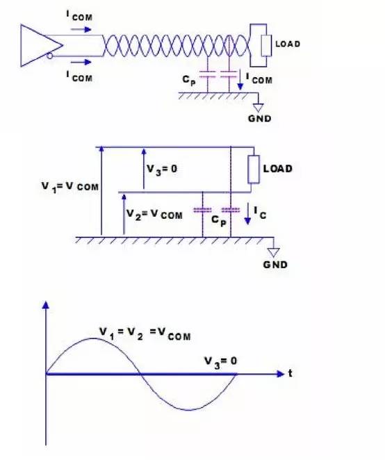
When the signal voltage (differential mode signal) is applied to the two legs of the transformer, the induced voltage is induced at the secondary side of the transformer through magnetic circuit coupling. For the signal voltage, since the signal currents flowing through the two windings of the CMC are equal in magnitude and opposite in direction, magnetic fluxes in opposite directions are generated in the core magnetic circuit of the CMC, cancel each other, and do not affect differential mode signal transmission. At this time, the Transformer Transformer flows through the two windings in the same size and direction, resulting in the Transformer acting as a large resistor, which hinders the passage of the differential mode signal and has little effect on the carrier signal transmission. So the differential mode signal is directly coupled to the load. For the common-mode signal, it is mainly coupled to the secondary through distributed capacitance between the primary and secondary of the transformer. At this time, the CMC and the two windings flow through equal-sized and same-direction currents. In this case, the CMC is equivalent to one. Large resistors prevent the transmission of common-mode currents, while transformer Transformer's two windings flow equal and opposite currents, and are short-circuited to the common-mode signal, so that the common-mode voltage is not substantially transmitted but coupled. To the load. Thus, the carrier signal can be transmitted well and the common-mode interference signal can be suppressed.
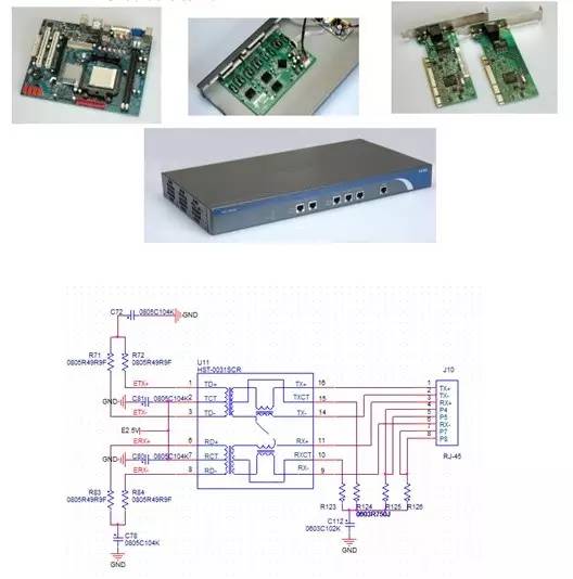
Transformer's center tap. Why the middle tap some access to power? Some ground? This is mainly determined by the use of the phy chip UTP (twisted pair) port drive type, there are two, if it is voltage-driven, then we have to connect the power supply; if it is current-driven it is not necessary to directly connect a capacitor to the ground. Why some 2.5v? And what about 3.3v? This is determined by the UTP port level specified in the PHY chip data. If it is 2.5v, it will pull up to 2.5v, if it is 3.3v, it will pull up to 3.3v.
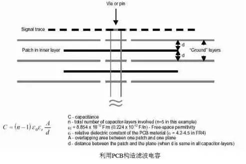
4, network transformer PCB design
Design Points:
First, create a noise-free, stable power environment
Second, reduce the impact of EMI, EMC on the chip
Third, simple signal wiring, reduce the length of the wiring

1. In the above figure, the module A (capacitor, resistor) should rely on the PHY as much as possible. Module B should be placed as close to the transformer as possible (because the RTL8201 draws current from Block A when it is transmitted, and the RTL8201 will collect differential signal voltage from Block B when receiving it.
2. The distance between the RJ-45 and the transformer (L1) should be shortened as much as possible.
3. The Rtset signal should be as close as possible to the PHY, and should stay away from TX+/-, RX+/-, and clock signals if possible
4. Crystals should not be placed near I/O ports, circuit board edges, and other high-frequency equipment, traces, or magnetic components. 5. The crystal case is well grounded to avoid external noise from EMC/EMI. Retaining straps of the crystal also require good grounding. 6. Magnetic components or components that generate magnetic fields should be isolated and maintained at 90 degrees to each other. High-current components should be placed close to the power supply to reduce traces. High current traces will create more EMI problems.
7. Terminator resistance: As described above for modules A and B, the resistance and capacitance of module A should be close to the PHY, and the two receiving termination resistors can be close to the transformer. For better impedance matching, these resistor/capacitor pairs should be carefully selected.
8. The distance between the PHY and the transformer (L2) should also be as short as possible. For practical convenience, this is often abandoned. However, it is very important to maintain the symmetry of Tx±, Rx± signal traces, and L2 needs to be kept within a reasonable range of about 10~300px.
Design example:
A, network port transformer is not integrated in the connector network port PCB layout, wiring rules
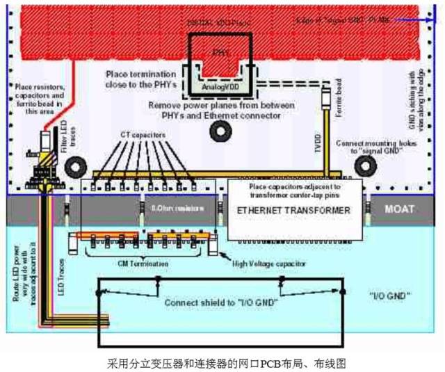
Referring to the figure above, note the following points:
1. Between the transformer and RJ45, the distance between the PHY layer chip and the transformer should be controlled within 1 inch. When layout conditions are limited, priority should be given to ensuring that the distance between the transformer and the RJ45 is within 1 inch.
2, the device layout according to the signal flow, do not go around.
3. The ground plane below the transformer should be divided. The width of the dividing line should not be less than 100 MIL. The network port transformer should be placed on the dividing line between GND and PGND.
4, each pair of differential traces must control the same length of the trace, while paying attention to the control impedance of 50 ohms
5. Note that the digital and analog grounds of the PHY chip are unified. The digital power supply and the analog power supply use magnetic beads for isolation. At the same time with the transformer. Pay attention to the power filter of the PHY chip and design it according to the chip requirements.
6. The network port indicator's power supply line 3.3V or 2.5V comes from the power plane. Use magnetic beads and capacitors for decoupling; the indicator drive line should be close to the PHY serial resistance and before entering the I/O area Capacitance filtering. This prevents noise from coupling to the differential line pair area through the indicator power line.
7. The indicator power line and drive signal line should be close to the line, so as to reduce the loop area as much as possible. See the lower left hand side.
8. The indicator line and the differential line pair must be isolated as necessary. The two should be far enough apart from each other if necessary to use the GND plane for isolation.
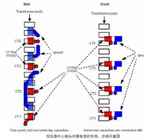
9. Pay attention to the filter capacitance of the central tap of the network port transformer chip to the ground as close to the transformer pins as possible to ensure the minimum inductance of the shortest trace distribution.
10. A 0 ohm resistor or capacitor used to connect GND and PGND should be placed on the ground divider.
11. The analog power supply of the PHY chip does not occupy a large area plane, and the local copper trace is pulled from the local copper trace through the trace, the magnetic beads, and the trace to the center tap of the transformer chip side.
12. There is no VDD between the PHY chip and the transformer. The plane layer area between the PHY chip and the transformer is defined as GND, which can cut off the noise path from the VDD plane. The actual processing is shown in the figure below.

13, along the edge of the PCB board (do not contain PGND, see Figure 8) hit a grounding vias every 250mil, these via rows can cut off the way the board noise radiation, reduce the impact on PGND static .
14. The PGND and GND of the board are connected through the boring holes and the structure to ensure the unification of the system ground potential.
15. Ensure good decoupling (low resistance) between the power plane and the ground plane. The power plane is preferably adjacent to the ground plane. 16. The signal line adjacent to the power plane should not exceed the projection area of ​​the power plane.
17. The integrity of the return path of the signal line adjacent to the power plane should be ensured. Otherwise, the shape of the plane must be changed so that the signal line is in the plane layer. The incomplete return path will bring serious EMC problems.
18. It is recommended that all high-speed signal lines, I/O lines, and differential line pairs be routed preferentially near the ground plane. If this cannot be achieved, use the power plane as the reference plane.
19. The differential line should be far away from other signal lines. Place other signal lines to couple the noise to the differential line. 20, in order to reduce the noise of the differential signal, digital signal line or power supply should be far away from the analog signal line or power supply.
21. Power supply decoupling and bypassing are very important. They can provide a low-impedance path for the signal and reduce the resonance between the power supply and the ground plane. Capacitance can act as a decoupling and bypassing, but to ensure that the decoupling and bypass capacitors by the capacitor, traces, vias, pads loop area as small as possible to ensure that the lead inductance is as small as possible, see below Shown:
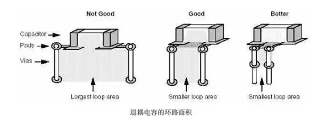
From the above figure, the rightmost case has the smallest loop area.
As can be seen from the above figure, in the layout on the left, the capacitor is connected to the plane through a long wire and there is a large lead inductance. In the right layout, the connection of the decoupling capacitor is very short, which ensures the requirement of low lead inductance.
B. PCB layout and wiring rules for network ports using integrated connectors
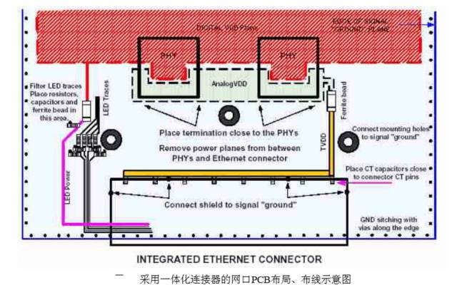
The integrated connector is more and more widely used because of its small size and good performance. Through practical application, it was found that the integrated connector can effectively reduce the EMI of the network port.
From the above figure, we can see that the difference lies in less network transformers, and most of the others are the same. The following description is only for different points.
1. The network port transformer is an isolation device that is used to cut off the common mode because it has been integrated in the connector, so the ground plane is no longer divided.
2. The housing of the integral connector should be connected to a continuous ground plane. Do not create chassis ground below the connector. 3. Ground the grounding via holes every 250mil around the board to shield the board's noise in the board.
C, power, ground layout
Although we have always recommended that power and ground planes be adjacent, some price-sensitive boards may not be able to do so. The following suggestions can reduce the impedance of the power supply to some extent. See below:
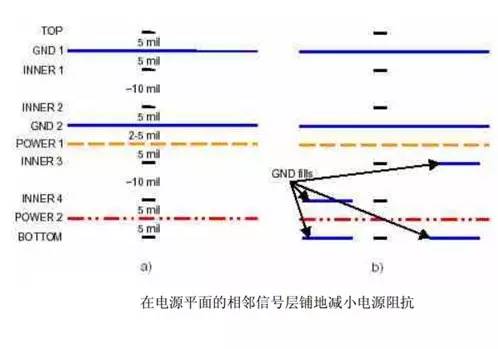
The power layer power2 is not adjacent to the ground plane, and the impedance to ground may be large. If the decoupling is unreasonable, it will bring EMC problems. Moreover, if the POWER2 layer is divided into multiple voltage regions at the same time, the signal lines across these regions will have a large loop area due to the discontinuity of the return path, resulting in EMC problems.
If we fill in the inner4 layer and bottom layer, we can reduce the impedance of the power supply to a certain extent, and create a low-impedance path for the signal line.
D, differential line pair layout, wiring requirements
Differential pairs exist in differential form and have strong common mode rejection. However, if the layout is not properly routed, the differential mode can be converted to common mode, causing common mode noise. Therefore, pay attention to the treatment of differential lines:
2. The distance between differential pairs must be the same, approximately equal to the line width. 3, the differential impedance of the line to control 100 ohm ± 10%. 4. It is advisable to route the inner layer and make it as close as possible to the ground plane.
5, to maintain the symmetry of differential pairs, any asymmetry will cause the differential mode to common mode.
E. Layout and wiring of differential signal termination resistors and filter capacitors
The 49.9 ohm terminating resistor (some PHY may not be available) must be placed close to the TX and RX pins of the PHY chip. The middle of the two terminating resistors must be connected to the ground as short as possible. As shown below:
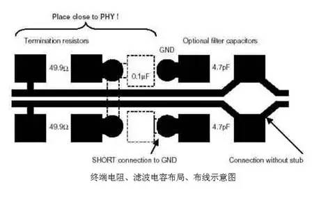
As shown in the above figure, the two 4.7 PF capacitors on the right have good suppression of high-frequency noise, but only the low inductance of the capacitor leads is ensured. The two filter capacitors must be well symmetric to ensure balance, otherwise the differential mode may be converted to common mode, causing common-mode noise. It is also important to note that the value of the capacitor should not be too large. A too large capacitance will affect the quality and even the function of the signal.
In addition, the two 4-7PF capacitors can be generated by a plane. As we all know, the distributed inductance of the planar capacitor is very low. In the signal layer adjacent to the ground plane, a patch is applied to the signal layer to generate a patch. High-performance capacitors. See below:
F. Transformer with high common mode rejection capability
The common-mode rejection capability of the transformer can reduce the transition from differential to common mode, but the common mode rejection performance within the scope of EMC testing is not generally listed in the transformer datasheet. This makes the choice of transformer difficult.
1. Select the transformer with common mode choke on the line side.
2. The use of a transformer that supports auto-negotiation may reduce the common-mode rejection capability. This type of transformer is symmetrical in its transmission and reception, and the center taps of the receiver and transmitter coils are connected together.
Common-mode resistors and high-voltage capacitors on the line side of the transformer
The 75 ohm resistors and high-voltage capacitors on the line side of the transformer provide common-mode paths for UTP cables. Note the layout and wiring considerations:
1. Place these common-mode resistors close to the center tap of the transformer.
2. Use short, thick traces (10 to 15 mils) for connection between resistors and capacitors. According to the different transformer structure, it can be mainly divided into the following two situations:
For the case of Figure 1 above, the value of the recommended resistor is 75 ohms, but the prerequisite for this is to ensure that the rack is quiet. For the case of Figure 2 below, the recommended resistor value is 0 ohms.
G, change the differential line number transmission waveform
Some PHY chips can change the rising and falling edges of a signal by setting a register inside a specific pin. A certain degree of slowing signal's rising edge (or falling edge) can reduce EMI by a certain length.

5, network port lightning protection circuit design
The lightning protection of the network port can adopt two kinds of ideas: One idea is to give lightning current to discharge the channel, discharge the high voltage before the transformer, minimize the impact on the transformer, and pay attention to reduce the common-mode over-voltage to poor Possibility of over-voltage. Another idea is to use the insulation voltage of the transformer to isolate the high voltage from the primary of the transformer through good device selection and PCB design, so as to achieve isolation protection of the interface. The following two solutions are adopted for the lightning protection circuit for the outdoor cabling network port and the lightning protection circuit for the indoor cabling network port, respectively.
Outdoor cable network lightning protection circuit
When there is a possibility of outdoor cabling, the protection level of the port is higher and the protection circuit can be designed as shown in Figure 7-8.
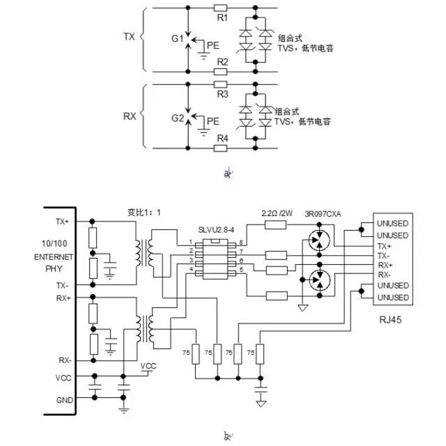
Outdoor route network port protection circuit
Figure a shows the basic circuit diagram of the protection circuit for the outdoor cabling network port. It can be seen from the figure that the structure of the circuit is similar to that of the outdoor cabling E1 port lightning protection circuit. The common mode protection is achieved through the gas discharge tube, and the differential mode protection is achieved through the secondary protection circuit composed of the gas discharge tube and the TVS tube. In the figure, G1 and G2 are three-pole gas discharge tubes, model 3R097CXA, which can simultaneously provide differential mode protection between two signal lines and common-mode protection of two lines to ground. The middle decoupling uses 2.2Ω/2W resistors, so that the front and rear stage protection circuits can cooperate with each other. The resistance value is selected as large as possible under the premise of ensuring signal transmission, and the lightning protection performance will be better, but the resistance value cannot be less than 2.2Ω. For the TVS tube for protection at the later stage, because of the high transmission rate of the network port, the combined TVS tube used in the network lightning protection circuit needs to have a lower junction capacitance. The recommended device model is SLVU2.8-4. Figure b is a detailed schematic of the network port portion of the device.
The middle pole of the triode gas discharge tube is connected to the protection ground PGND. It must be ensured that the working ground GND and the protection ground PGND of the equipment are connected to the structure through the PCB traces on the motherboard or through cables (do not pass 0Ω resistance or capacitance). In order to reduce the potential difference between GND and PGND, the lightning protection circuit plays a protective role.
The circuit design needs to pay attention to the PCB trace from RJ45 connector to triode gas discharge tube is thickened to 40mil, and the trace is laid in the TOP layer or BOTTOM layer. If a single layer cannot be covered with such a thick line, two or three layers can be used to meet the width of the trace. The decoupling resistor to the PCB trace of the transformer is recommended to use a 15 mil line width.
The insertion loss of the lightning protection circuit is less than 0.3dB, and the impact on the transmission signal quality of the 100M Ethernet port is relatively small.
Indoor cable network lightning protection circuit
When only indoors, the protection requirements are low, so the lightning protection circuit can simplify the design, as shown in the figure, a is the basic principle diagram of the indoor routing network protection circuit, Figure b is the protection device selection SLVU2.8- The detailed schematic of the 4 port network port.
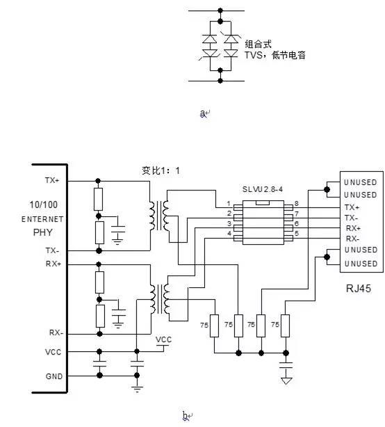
Indoor route network port protection circuit
The Ethernet signal cable of RJ45 connector is balanced twisted pair, and the induced lightning overvoltage is based on common mode. If overvoltage can be effectively protected, the differential mode protection can be selected with a small amount of devices, usually Select SLVU2.8-4, it can achieve differential mode 0.5kV (1.2/50us) protection, but when the product target includes the North American market, the differential mode protection device is recommended to use LC03-3.3, which can meet the NEBS certification requirements.
We compare these two circuits in terms of common-mode protection. The outdoor circuit adopts the gas discharge tube to achieve the protection of the common mode. When a common mode overvoltage is generated at the port, the gas discharge tube is converted into an overcurrent and discharged, thereby achieving the purpose of protection. The network port protection circuit in Figure 7-9 only designs the differential mode protection circuit, and does not have a common mode protection circuit. It uses the common mode protection of the port. It is the isolation protection concept that we mentioned earlier. It uses the network. The isolation characteristics of the port transformer allow port common mode protection. When overvoltage occurs at the port, this overvoltage will be added to the primary of the network transformer. Because the transformer has certain isolation characteristics, as long as the overvoltage does not exceed the withstand voltage capability of the transformer primary and secondary, it is broken down. It will be completely isolated on the primary side, so that it will not affect the secondary side basically and achieve the purpose of port protection.
It can be seen from the above principle that the common mode protection of such a circuit in indoor protection mainly depends on the PCB traces of the transformer front stage and the insulation voltage of the transformer. Therefore, strict attention must be paid to the selection of the device and the design of the PCB.
First of all, in the design of the Ethernet port circuit should establish a sense of separation of high-voltage lines and low-voltage lines. Among them, the Ethernet differential signal line and the Bob-Smitch circuit on the external side of the transformer are directly connected to the RJ45 connector, and it is easy to introduce external overvoltage (such as lightning induction, etc.), which belongs to the high voltage signal line. The pilot line, power supply, and GND are provided by the system and belong to the low-voltage line.
According to the different network port connectors, the network port circuit is divided into two kinds: with or without a lamp. Among them, the lightning protection problem of the network port with a lamp connector is more prominent. Therefore, the following takes the network port lamp circuit as an example to illustrate How to distinguish between high voltage lines and low voltage lines.
The typical circuit with a network port is shown in the figure below:
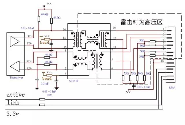
Network port part of the circuit
When an online lightning cable experiences an induced lightning strike, overvoltage will be generated on the eight network cables at the same time. From the perspective of security, the network port should be divided into high-pressure area and low-pressure area. As shown in the above figure, the high-pressure area is in the dotted line frame. Therefore, when the lightning induced by the network cable is mainly in the high voltage area, there is a relatively high overvoltage. However, in the high-voltage zone, only 8 network cables and the connected network are high-voltage cables, while the indicator lamp driving line, 3.3V power supply, and PGND of the connector housing are low-voltage cables. The matching resistance of the network cable Bob-Smith circuit is high voltage. The current limit resistor of the indicator is in the low voltage range. One end of the middle tap capacitor on the transformer cable side is the high voltage end, and the other end connected to PGND is the low voltage end.
Secondly, the network port lightning protection circuit should pay attention to the following points in the device selection and PCB design process:
In order to ensure the withstand capability of the common-mode isolation withstand voltage, the transformer needs to meet the AC insulation voltage withstand voltage between the primary and secondary is not less than AC1500V.
The RJ45 with no lamp is preferred. If the lamp is to be led, it is recommended that the light guide be used to guide the light of the indicator to the panel on the side of the chip to prevent the control signal of the indicator from crossing the area where the high voltage signal line and the Bob-Smitch circuit are located.
The current limiting resistor of the indicator lamp control circuit should be placed on the control chip side, close to the control chip, to prevent the overvoltage from directly impacting the control chip.
The Ethernet signal line follows the rules of differential line routing to ensure impedance matching, and the length of a pair of differential lines is as long as possible.
If the transformer pre-stage (on the RJ45 connector side) has a center tap and uses a Bob-Smith circuit, ie a 75Ω resistor plus a 1000pF PGND-connected capacitor. It is recommended that the capacitor should have a withstand voltage greater than DC2000V. A single resistor of 1/10W is recommended for resistor power.
An Ethernet interface uses a Bob-Smitch circuit to avoid multiplexing the Bob-Smitch circuits of multiple Ethernet interfaces.
For a board with more than 6 layers of PCBs, since the insulating material of adjacent layers is less than 12 mils, the high-voltage and low-voltage wires should not be laid on adjacent layers, and should not be crossed or drawn close to each other.
Because common mode protection is achieved through the isolation characteristics of the transformer, sufficient insulation between the high voltage signal lines (differential lines and Bob-Smitch circuit traces) and other signal lines (indicator control lines), power lines, and ground lines should be ensured. There is no accidental discharge route.
Finally, to achieve effective isolation between the high voltage and low voltage areas, we must pay attention to the PCB trace design between the two. In high voltage areas, with high voltage may include: connector pins, wiring, vias, resistance pads, capacitor pads. With low voltage may be: wiring, vias, resistance pads, screws. According to the test results and analysis, we obtained the insulation withstand voltage data between the high voltage and low voltage types of the various types of PCBs in the net port PCB, as detailed in the following table (the table shows the pressure resistance when the distance between the high voltage and low voltage parts is 10mil. Happening):
Insulation pressure test results
| High pressure | RJ45 connector pins | PCB trace | Via | Pad | |
| resistance | capacitance | ||||
| PCB trace | Infer >2200V | Infer >2200V | 2200V (inner layer) | 1200V (surface) | Inferring 1200V |
| Via | —————— | Infer >2200V | 1000V | 1500V (recommended for 750V design) | 750V |
| Resistance pad | —————— | —————— | —————— | ---- | ---- |
| Screws | —————— | 1000V | Inferring between 320V and 750V | Infer >320V | 320V |
| Transformer pins | 1250V |
Note: The red data in the above table is obtained by direct test, and the black number is based on the test and analysis of specific conditions. The blue data is the principle analysis data. It is recommended to design according to this value during the design process.
It can be seen from the table that, for the same insulation distance, the withstand voltage capability is ground screw <capacitance, resistance pad <via trace <surface trace <inner trace, so when the common mode protection index is fixed, high voltage The insulation distance between the part and the low-voltage part should be ground screw> capacitance, resistance pad> trace via> surface trace> inner trace. This is because the entire screw is a metal body, and the exposed area is relatively large, and it easily becomes a discharge path. Both surfaces of the capacitor and the resistance welding are metal, and since the shape is a rectangular parallelepiped, angular, it is easy to form a tip discharge. There are many via holes in the network port, the surface is bright tin, but also easy to produce breakdown discharge, but compared with the resistance and capacitor welding ends, the metal area is relatively small. The surface of PCB board is coated with insulating green oil, and the inner layer is surrounded by medium. Compared to the above, the withstand voltage capability should be higher.
In the design, according to the surge resistance rating of specific product requirements, using the data in Table 7-1, we can calculate the various insulation distances that PCB design needs to control. The safe insulation distance that the PCB design should achieve when the protection level is 4kV is given.
| High pressure | Connector Pins | line | Via | Pads (capacitors, resistors) |
| line | 20mil | 20mil | 20mil | 33mil |
| Via | ---- | 20mil | 40mil | 53mil |
| Screws | ---- | 40mil | 120mil | 120mil |
Table PCB design safety insulation distance data (calculated according to 4KV withstand voltage)
In summary, using the protection circuit in the figure, through a good device selection and PCB design, can achieve common mode 2kV (1.2/50us, up to 4kV), differential mode 0.5kV (1.2/50us) protection . It can be used in most indoor cabling situations, especially for access and terminal equipment. In actual use, the Ethernet cable does not use shielded cable, and the installation and use length is more than 50 meters. In the process of designing the protection circuit of the network port The above issues should be taken seriously.
For the protection of the network port, in addition to the above two circuits in Figure 7-8 and Figure 7-9, there is the use of RJ45 connector pin front discharge design, the use of transformer center tap air discharge design and the use of the transformer center tap Discharge tube discharge design and other protection methods are characterized by the use of insulation discharge to achieve protection, low cost, PCB footprint is small.
Other questions and answers:
In an Ethernet device, when a PHY is connected to RJ45, a network transformer is added in the middle. Some transformer center taps are connected to ground. And when the power supply is connected, the power supply value can be different, 3.3V, 2.5V, and 1.8V are all available. The role of this transformer is analyzed as follows:
Why the middle tap some access to power? Some ground?
This is mainly determined by the type of UTP port driver used with the PHY chip. There are two types of drive, voltage-driven and current-driven. The voltage drive must be connected to the power supply; the current drive can directly connect the capacitor to ground! Therefore, for different chips, the center tap connection is closely related to the PHY. Specifically, please refer to the chip's datasheet and reference design.
Why connect different voltages when connecting to the power supply?
This is also determined by the UTP port level specified in the PHY chip data used. The decision of what level, you have to take the appropriate voltage. That is, if it is 2.5v, it will be pulled up to 2.5v, if it is 3.3v, it will be pulled up to 3.3v.
3. What is the role of this transformer in the end, can we not take it?
In theory, it is possible to connect to RJ45 directly without the need of a transformer, and it can also work normally. However, the transmission distance is very limited, and it will also have an impact when it is connected to a different network port. And the external interference to the chip is also great. When connected to a network transformer, it is mainly used for signal level coupling. First, the signal can be enhanced to make the transmission distance farther; second, the chip end is isolated from the outside, the anti-interference ability is greatly enhanced, and the chip is greatly protected (such as a lightning strike); If you go to a network port with different levels (for example, some PHY chips are 2.5V and some PHY chips are 3.3V), they will not affect each other's equipment.
Which size you prefer when looking for an android tablet for students take online learning? 10 inch android tablet, 8 Inch Tablet , 7 Inch Tablet, or others? Frankly speaking, 8 inch android tablet is the most competitive student tablet, no matter size, lasting time, screen size, cost, etc. Therefore, 8 inch android tablet price is the device balancing quality and cost at top. Of course, 5g android tablet also available as well. As a professional manufacturer, more designs are under-developing, you can also share the design, parameters needed, then our team customs for you.
The another target clients is the reselling or importing wholesales. So if you are doing android tablet deals, this store also brings surprise when take a deep checking, not only different size education tablet, but also windows tablet, or tablet 2 In 1 Laptop with android os or windows OS.
Except tablets, you can also see 14.1 inch celeron Education Laptop, 15.6 inch celeron business laptop, 15 inch Gaming Laptop with intel core i3, i5 or i7, 16.1 inch i7 16gb ram 4gb graphics laptop, etc.
Android Tablet,10.1 Android Tablet,Android Tablet Price,5g Android Tablet,Android Tablet Deals
Henan Shuyi Electronics Co., Ltd. , https://www.shuyilaptop.com