In modern air combat, optoelectronic countermeasures equipment plays an important role in the war, and the infrared detection and tracking system uses passive detection technology, so it has strong stealth and anti-interference ability compared with active detection systems such as radar. The advantages of high degree of miniaturization have attracted the attention of the industry. The new generation of infrared imaging guidance system must have high precision, fast processing speed, strong real-time performance and short response time. This requires the image processing computer to meet the large data volume, complex calculation, real-time and high transmission in image processing. Rate and stability and other requirements. In this paper, the design method of infrared information data processing system based on DSP and FPGA chip is introduced from three aspects: working principle, hardware and software.
1Infrared guidance control system hardware overall design
The infrared information data processing system is divided into two sections according to functions, and the image information processing board and the control information processing board form a data processing system. Its infrared guidance control information data processing system is shown in Figure 1. The image information processing board mainly undertakes a large number of real-time image signal preprocessing, image signal processing and control tasks; control information processing board control interface signal acquisition, tracking loop solution, control output and communication with the flight control computer, etc., while controlling The management module is also the management module of the system, and completes functions such as input/output operation, synchronization control, and system state management of the system.
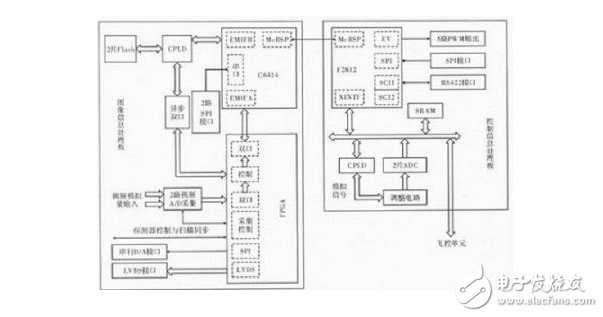
Figure 1 Infrared information data processing system block diagram
2 hardware design of image processing module
The hardware of the image processing module is composed of a reset circuit, a clock circuit, an image acquisition and preprocessing circuit, a DSP image processing circuit, a power conversion circuit, and an external interface. The block diagram of the composition is shown in Figure 2.
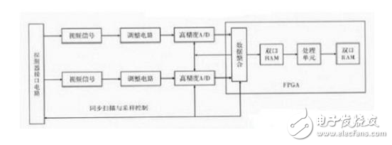
Figure 2 image acquisition unit circuit composition
2.1 image acquisition unit
The image acquisition unit comprises a scan synchronization interface circuit, a detector interface circuit, a front end adjustment circuit, an A/D conversion circuit, a sampling control and data integration circuit, and a data buffer (synchronous dual port) circuit. The block diagram of the circuit is shown in Figure 2. The scan sync signal is from a scanning module in the system that provides a system timing reference whose signal is synchronized to the frame sync signal. The scan sync signal is accessed from the backplane connector. The detector interface circuit includes: a reference power supply, a temperature signal, a sampling control signal, and two video analog signals. The above signals are controlled by the internal acquisition circuit of the FPGA to ensure synchronous acquisition of image data per frame. The adjustment circuit adjusts the video signal output by the detector to the range of the high-speed A/D input. The differential video signal is amplified by a differential driver. The common-mode input voltage is the video A/D on-chip reference signal (2.5 V). Analog signal input to A/D uses differential input. Video A/D is mainly used to convert analog signals and digital signals between video circuits. According to the overall requirements of the circuit, the A/D conversion circuit needs to meet the requirements of high sampling frequency, low power consumption and high conversion accuracy. The sampling control and data buffer circuits are implemented by the FPGA internal sampling control circuit. The data buffer circuit is implemented by the FPGA's internal dual-port memory and has high-speed, synchronous and asynchronous read and write operations.
2.2 DSP image processing circuit
The DSP image processing circuit mainly includes a processor and a peripheral configuration circuit, a memory circuit, and a McBSP serial port circuit that communicates with the control board interface. The processor selects C6414 GIZA-6E3 from TI's high-performance fixed-point TMS320C641x series as image information processing C6414-6E3 with clock period of 1.67 ns, internal working clock up to 600 MHz, maximum processing speed of up to 4 800 MIPS, and internal memory capacity of 8 Mbit; has 2 extended memory interfaces, EMIFA is 64 bit, EMIFB is 16 bit, EMIFA bus frequency can reach 133 MHz, maximum addressable space is 1280 MB; core working voltage is 1.4 V, working temperature can reach -40 ~105 ° C. It completes the main processing algorithms such as image combination, segmentation and enhancement, template matching, background processing, target extraction and target tracking of infrared imaging guidance seeker.
The FPGA pre-processing unit is another core component on the image information processing board, which is implemented by XC2V2000-FG676 in the Xilinx Vertex-II series. The XC2V2000 has a size of 2 million gates. The internal storage resources include 1 Mbit of Select RAM, 336 kbit of Distributed RAM, IO pin resources of 408, and 8 DCM. The FPGA preprocessing unit is designed by the video acquisition control and data integration unit. Video capture buffer and main processing buffer dual-port memory, pre-processing unit, image output daughter card data transmission interface control, serial SPI interface controller, LVDS digital video output interface, host control circuit for accessing DSP/HPI interface, etc. . In addition, the FPGA configuration of the image information processing board can realize the external field online configuration function.
The memory circuit includes two kinds of memories: Flash and FPGA internal synchronous dual port. It can be connected with C6414 (EMIF external memory interface, C64 has 2 bus EMIFA and EMIFB). In use, the EMIF bus needs to be configured by DSP/BIOS to determine the access timing. There are two flash resources on the image information processing board belonging to DSP and FPGA respectively. The Flash belonging to the FPGA saves the on-board control code. The Flash belonging to the DSP can store the user application in addition to the storage module BOOT program. In order to adopt the slave mode configuration FPGA, the Flash connected to the C6414 EMIFB asynchronous BANK CE0 adopts asynchronous read/write signals; in order to support the C6414 boot mechanism from the ROM, the DSP belongs to the EMIFB asynchronous BANK CE1 connected to C6414. Read and write signals. The dual port memory is mainly used to store frame image data, and a dual port memory is configured on the FPGA of the image information processing board. In the application, synchronous or asynchronous dual-port memory can be used to exchange data with C6414 through FPGA design. The capacity can be configured as 16 kbit & TImes; 16 bit, or 16-bit or 32-bit access mode. The dual-port memory on the image processing board is connected to the EMIFA synchronous BANK ACE0 space of the C6414, which can be configured in synchronous mode or asynchronous mode.
3 control information processing module hardware design
The control information processing board is composed of a processor, a clock and a reset circuit, a memory, a digital pulse counting and logic control circuit, an analog-to-digital conversion A/D circuit, and an indicator circuit. As shown in Figure 3.
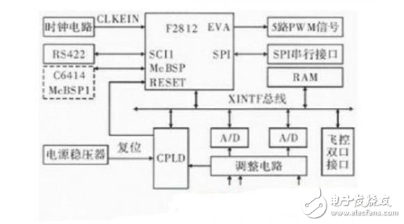
The control information processing board signal processor uses the TMS320F2812, which provides an input operating clock from a 30 MHz crystal, 16-bit bus width, 128 kW of on-chip program memory and 64 kW of data memory, and three levels of external interrupts. The clock circuit uses an external crystal to provide a 30 MHz clock input to the F2812. The internal PLL circuit is configured with an F2812 operating clock of 120 MHz and an external bus operating clock of 60 MHz. The reset circuit is output by the LDO power converter of this board, and the reset input is via the CPLD. The logic control generates a reset of the control information processing board DSP. The control information processing board mainly has the following memory configurations: F2812 on-chip memory includes: 18 kW SARAM, 128 kB Flash, 4kB Boot Rom. Off-chip memory space includes: 512kB SRAM, 1 kB flight control computer dual port storage The data register of the space, the 3-channel digital pulse counting circuit, and the data port address of the two A/D converters on the board.
The programmable logic CPLD circuit completes the three digital pulse counting, reset circuit and decoding logic of the control information processing board. The decoding logic is generated by the external memory chip select signal of F2812 and the upper address line together to generate access A/ by logic decoding. D chip and chip select signal interfaced with the flight control module.
CPLD realizes the principle of counting and frequency measuring three digital pulse signals; the three digital pulse signals are counted by the CPLD frequency measuring circuit, and then read by F2812 through software programming.
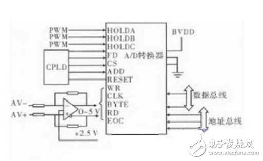
Two A/D converters implement analog-to-digital conversion of 9 analog inputs. The A/D circuit is shown in Figure 4. The system inputs 9 differential AC analog signals. These 9 analog signals need to be adjusted to 0~+ using differential op amps. 5 V, input to the A/D converter at the same time, the sampling clock is controlled by the CPLD.
4 software function design
The image control information processing system has a complicated structure and a large number of interfaces. Due to space limitations, only a brief introduction to the BIT test method to verify whether it meets the imaging guidance system and target signal processing system specifications is given. The A/D test uses the digital FFT method. The Flash and RAM tests are performed by comparing the on-chip spatial data with the read and write. The interface test is performed by inputting the analog signal from the external interface through the hardware interface, and the software is used to judge the operation result by threshold value. The data transfer rate test is implemented by the EMIF bus and the synchronous dual port RAM configuration inside the FPCA as the master-slave test loop method. The BIT test result is transferred to the RS232 interface through the RS422 interface and connected to the PC display. The test results show that the local circuit is faulty and easy to locate.
5 Conclusion
In this paper, the data processing system is developed based on the DSP (TMS320C6414) processor + FPGA (XC2V2000-FG676) as the core of the infrared image information processing of the missile computer. The software and hardware design is carried out. The test results show that the system has strong processing capability, convenient debugging, and easy positioning when hardware failure occurs.
MC Plus series LED Light Box
Product categories of LED light Box includes MC Plus series Indoor LED Light Box and MC Plus series Outdoor LED Light Box. Led Advertising Machine, Outdoor Led Poster, Floor Standing Outdoor Led Poster suppliers/factor.
LED Light Box as an advertising form of new media, transcending the limits of time and space, transmits multi-media information to realize personality and customization service. Outdoor led poster (led light box) is a very effective, eye-catching medium which can be fabricated as per the requirement of the application. led light box can be used to welcome guests, advertise products as well as disseminate important information relevant to its viewers.
Moreover, led light box can be used for advertisement but also the weather information and other tasks like online surfing, bill payments, shopping, etc.
LED Light Box
LED Light Box,Acrylic LED Light Box,LED Advertising Light Box,LED Window Light Box
Shenzhen Macion Optoelectronics Technology Co.,Ltd. , https://www.macion-led.com