The rapid development of electronic technology has placed higher demands on electronic instruments and equipment. Modern devices are expected to be more secure, reliable, and feature-rich, while also becoming more automated and compact in size. This has led to the increasing use of switching power supplies in various fields such as computers, telecommunications, aerospace, and color TVs. However, the switching transistors in these power supplies operate in a switching state, generating strong peak and resonance interference through circuit components. These electromagnetic interferences (EMI) can severely pollute the utility grid, disrupting nearby electronic devices. Moreover, due to this issue, switching power supplies are not suitable for some high-precision applications. Therefore, minimizing EMI is essential to expand their usability, making it a critical consideration in the design of switching power supplies.
In this paper, we apply the principle of two-port networks to analyze the DC EMI filter used in switching power supplies. We provide a general method for designing DC EMI filters along with calculations for key parameters.
### 1. Design of DC EMI Filter Based on Two-Port Network
Switching power supplies, whether single-bridge, push-pull, half-bridge, or full-bridge, can generally be represented in the form shown in Figure 1 (for a single-phase configuration).
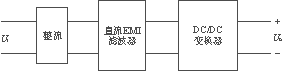
From this figure, it is clear that by incorporating a DC EMI filter, the equivalent impedance of the circuit can be modified to achieve the desired filtering effect.
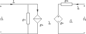
The DC EMI filter can be modeled as a two-port network, with the following mixed parameter equation:
$$
\begin{bmatrix}
I_1 \\
I_2
\end{bmatrix}
=
\begin{bmatrix}
g_{11} & g_{12} \\
g_{21} & g_{22}
\end{bmatrix}
\begin{bmatrix}
V_1 \\
V_2
\end{bmatrix}
$$
Where:
- $ g_{11} $: Input admittance
- $ g_{22} $: Output impedance
- $ g_{12} $: Reverse current gain
- $ g_{21} $: Forward voltage gain
The equivalent schematic of the DC EMI filter is shown in Figure 3.
The design of the DC EMI filter must meet the following requirements:
1. Ensure that the filter does not affect the load capacity of the power supply.
2. For the DC component, the filter should introduce minimal attenuation.
3. For harmonic components, the filter should provide effective suppression.
Based on these requirements, the input admittance $ g_{11} $ and output impedance $ g_{22} $ should be as small as possible, ideally zero. At low frequencies, $ g_{12} = g_{21} = 1 $, while at high frequencies, all parameters should be minimized to ensure optimal filtering performance.
### 2. Case Analysis
In engineering practice, common filters include LC filters and fourth-order DC line filters. Let’s examine the performance of an LC filter, as shown in Figure 4.
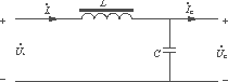
The mixed parameter equation for the LC filter is:
$$
\begin{bmatrix}
I_1 \\
I_2
\end{bmatrix}
=
\begin{bmatrix}
g_{11} & g_{12} \\
g_{21} & g_{22}
\end{bmatrix}
\begin{bmatrix}
V_1 \\
V_2
\end{bmatrix}
$$
At low frequencies ($ \omega \to 0 $), $ g_{11} = g_{22} = 0 $ and $ g_{12} = g_{21} = 1 $. For high-frequency harmonics, the values of $ g_{11}, g_{12}, g_{21}, g_{22} $ should be as small as possible. However, achieving this often requires large inductances and capacitances, which may limit practical application.
A fourth-order DC line filter, widely used in engineering, is shown in Figure 5.
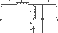
Its mixed parameter equation is:
$$
\begin{bmatrix}
I_1 \\
I_2
\end{bmatrix}
=
\begin{bmatrix}
g_{11} & g_{12} \\
g_{21} & g_{22}
\end{bmatrix}
\begin{bmatrix}
V_1 \\
V_2
\end{bmatrix}
$$
With $ g = \frac{1}{R} $ and $ z = j\omega L $, the parameters can be calculated accordingly.
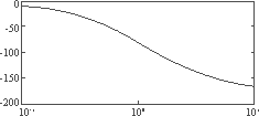
Using MATLAB, the logarithmic amplitude-frequency characteristic curve of the filter is plotted (Figure 6), showing good high-frequency attenuation and minimal low-frequency loss.
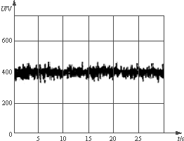
This design was applied to a switching power supply developed for a company in Changsha, meeting the following requirements:
1. Input peak voltage of 1000 V, maximum current of 20 A.
2. Voltage fluctuation of 513 V should not exceed 2% when output current changes from 0 to 25 A.
The selected parameters were:
- $ L_1 = 500\mu H $
- $ L_2 = 140\mu H $
- $ R_0 = 0.3\Omega $
- $ C_1 = 470\mu F $
- $ C_2 = 40\mu F $
These values satisfied the design criteria, resulting in improved output waveform stability, as shown in Figure 7.
### 3. Conclusion
By applying the two-port network principle, this paper analyzes and summarizes the design requirements for EMI filters in switching power supplies. The three main design criteria—low input admittance, high forward voltage gain, and low output impedance—are universally applicable to any filter design. Using these principles, we designed and implemented an EMI filter that demonstrated excellent performance in real-world applications. The results confirm that the theoretical approach is both practical and widely applicable.
Nickel Cadmium Alkaline Battery
Taihang Power begin to produce rechargeable battery since 1956, our Nickel cadmium battery capacity range is from 10ah to 1200ah. NICD battery has the properties of rigid construction, long service life,wide work temperature, resistance to overcharge and overdischarge, low self-discharge, high reliability and easy maintenance.
They are widely used as DC power source for railway vehicle, rolling stocks, petrochemical, oil and gas, electricity industries,electrical appliance,telecommunications, UPS, military, AGV,electric power system,wind and solar energy storage system,etc.
Nickel Cadmium Rechargeable Battery,Nickel Cadmium Alkaline Battery,Alkaline Nicd Batteries,Nicd Battery For Ups
Henan Xintaihang Power Source Co.,Ltd , https://www.taihangbattery.com