Abstract: The article analyzes the principle of the audio detection circuit. The audio signal passes through the detection circuit and triggers the output low level, so that the system automatically switches to the AUX (auxiliary input) signal source for playback.
Keywords: voltage following; filtering; amplification
0 Introduction At present, car audio functions are more and more, from radio, CD to DVD, Bluetooth, navigation and other functions, while AUX (auxiliary input) is also a must-have function, it can drive the user's portable audio equipment such as MP3, The iPOD is input to the car audio for playback. The automatic detection and playback circuit of the design is analyzed and explained.
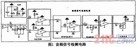
1 circuit composition This circuit consists of 6 parts: power circuit, voltage follower circuit, voltage inverting amplifier circuit, low-pass filter circuit, comparison circuit, detection output circuit. The circuit diagram is shown in Figure 1:
This article refers to the address: http://
2 circuit analysis
2.1 Power Circuit The power supply consists of 8V and 4V. 8V is the power supply for the op amp. At the same time, the bias voltage of the op amp is 4V by R13 and R14, and the input bias voltage of the four op amps is provided.
2.2 Voltage follower circuit In the voltage follower circuit, the operational amplifier IC1 and IC2 act as a voltage follower, superimposing the signal of the DC offset on the positive signal input end, and transmitting to the next stage without change. The input impedance of the op amp voltage follower is large and the output impedance is small. Since the input impedance is large, the input voltage is transmitted to the op amp with almost no loss, and the output impedance is small, and the output signal is almost completely transmitted to the subsequent circuit. The op amp has a good buffering effect, which blocks the influence of the latter stage on the input signal.
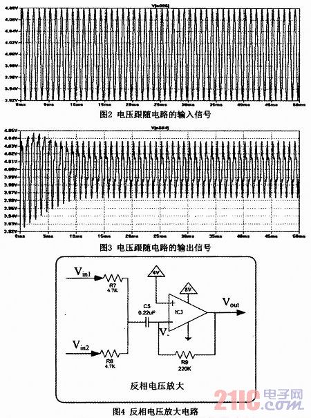
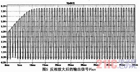
Simulated with a 80mV/1kHz sinusoidal signal in PSPICE, the input and output signals of the follower circuit are shown in Figure 2 and Figure 3.
2.3 Inverting Voltage Amplifying Circuit The circuit diagram is shown in Figure 4.
The amount of amplification of the AC signal by this circuit (where R7 = R8) can be derived from the following formula:
(VIN1-V-)/R7+(VIN2-V-)R8=(V--VOUT)/R9 (1)
VOUT=VIN1(-R9/R7)+VIN2(-R9/R8) (2)
VOUT=(VIN1+VIN2)(-R9/R7) (3)
VOUT/(VIN1+VIN2)=-R9/R7 (4)
For the AC signal, the bias voltage can be treated as ground, and the amplification factor of the inverting amplifier can be adjusted by equation (4) (R9/R7=220k/4.7k=46.8 is about 33.41dB), which can be changed. Detect the sensitivity of the circuit. The larger the absolute value of the amplification factor, the smaller the amplitude of the signal that can be detected, that is, the higher the sensitivity, usually the input of AUX is greater than 100mV, and the simulation uses 80mV as the input signal. When the input signal is large, that is, the inverting amplifier circuit is clipped, and there is no influence on the detection function. From the following rectifier circuit principle, it can be known that the upper part of the output signal acts on the rectification, and when the upper signal is clipped, It indicates that the output upper limit of the op amp has been reached, the amplitude is definitely greater than the unclipped signal, and this circuit is only the detection function, and does not need to take into account the distortion of the signal. Therefore, when the clipping phenomenon occurs, the detection function of this circuit has no effect.
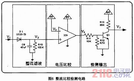
C5 is a countermeasure against low-frequency noise interference. After adding C5, in the amplification factor R9/R7 of the inverting amplifier, R9 is still (220k Ω), and R7 is synthesized by C5 (0.22 μF) and 4.7kΩ. of. The capacitive reactance of the capacitor is 1/(j*w*C). For low-frequency signals, the capacitive reactance is very large, and the high-frequency signal is close to short-circuit, so that the amplification factor of the low-frequency signal is greatly reduced, and for the high-frequency signal amplification factor is almost The same, it plays a role in suppressing low-frequency interference signals and prevents false triggering. Figure 5 shows the output of the circuit in the PSPICE after the 80mV signal is amplified:
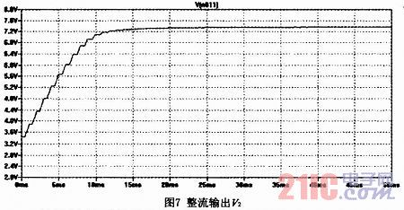
2.4 Rectifier Circuit The rectifier circuit consists of D1, R10, and C6 (see Figure 6). It acts as a gradual amplification of the signal, making it close to the DC signal. When the voltage difference between V1 and V2 is greater than the turn-on voltage of the diode, the diode conducts, charging capacitor C6 (while a portion of the current flows through R10 and the input impedance of the comparator); when the voltage difference between V1 and V2 is less than that of the diode When the voltage is turned on, the diode is turned off and the charge on the capacitor is discharged through R10 (and the input impedance of the comparator). When the voltage difference discharged to V1 and V2 is again greater than the turn-on voltage of the diode, the diode is turned on and the charging process begins. This circuit repeatedly performs such a charge and discharge process. Since the values ​​of R10 and C6 are both large, the discharge speed is very slow, and the capacitor voltage is close to DC. It can be obtained by the differential equation, the discharge time T = RC1n (Vo / Vt), Vo is the initial discharge voltage, Vt is the voltage after discharge, R is the resistance value of the discharge path, and C is the capacitance value of the discharge. It can be seen that the larger R, C, the longer the discharge time, that is, the voltage is less likely to change. Figure 7 shows the simulated output of the rectification filter.
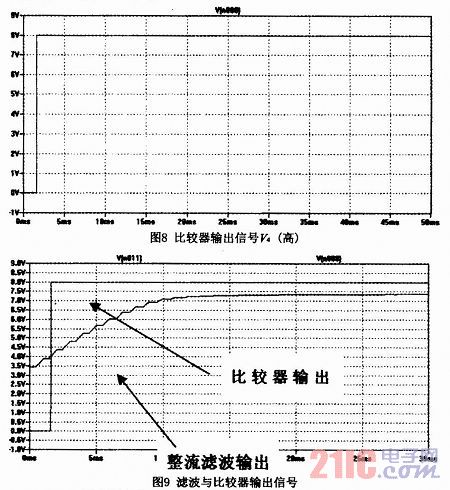
2.5 Comparison circuit The rectified and filtered signal V2 is input to the positive signal terminal of the comparator IC4 and compared with the negative terminal voltage of IC4 (V3=Vcc/2=4V). When the signal level value is greater than 4V, the comparator outputs a high level (V4 is close to the power supply of the op amp 8V). When the signal level value is less than 4V, the comparator outputs a low level (V4 is close to 0V). The flat will control the rear stage detection circuit. Figure 8 shows the AUX input signal and the analog output of the comparator output high level. Figure 9 shows the simulation output signal of the filter and comparator.
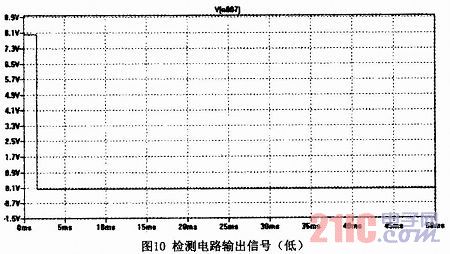
2.6 Detection Output After the comparator output is high, the transistor Q1 is turned on, that is, the Q1 collector output is pulled low, and the circuit output V5 is low. In this design, setting the low level to be valid means that the AUX has an audio input.
Referring to Figure 10, the simulation outputs a low level signal:
When the comparator outputs a low level, Q1 is turned off, and 8V is divided by R13 and the input impedance RMCUIN of the corresponding port of the micro control chip (MCU). Usually, the input impedance of the corresponding port of the MCU is RMCUIN ≈ 50kΩ, then the output high level can be as follows Calculated: ![]()
The circuit outputs a high level of 5V, and the MCU detects high, and it is judged that AUX has no signal input.
In this way, after the MCU detects the low level signal, it will automatically switch the sound source from CD or radio to AUX input, and automatically play the AUX signal.
3 Summary This circuit is simple and effective, can be applied to car audio products, automatic detection and playback, improving the user experience.
Solar Pv Test Equipment,Photovoltaic Testing Tools,Solar Iv Tester,Solar Pv Testing Kit
Sowell Electric CO., LTD. , https://www.sowellsolar.com