A programmable current limit circuit applied to a linear regulator (LDO) is proposed to achieve accurate sampling of the adjustment tube current. According to different operating conditions of input-output differential voltage and load current, the current limit value can be changed by adjusting the current-limiting resistor outside the chip. Based on the TSMC 0.25 μm BCD process, the simulation was performed using H-spice. The simulation results show that the LDO achieves a maximum output of 3 A load capacity within an input voltage range of 2 V to 5.5 V and an output voltage of 1.2 V to 5 V. The programmable current limit circuit can limit the current to 0.2. A~4.5 A programming.
0 Preface
With the popularity of portable electronic products, low-dropout linear regulators (LDOs) and switching voltage regulators are increasingly used. Switch-mode voltage regulators are very efficient, typically up to 90%. However, since the switching regulator needs an inductor, it is difficult to integrate and the cost is increased, electromagnetic interference (EMI) is also introduced, and the output ripple and noise of the switching regulator are relatively large and are not suitable for the output voltage requirement. More stringent occasions. Compared with switching regulators, LDOs have the advantages of low output voltage ripple and noise, and occupy less chip area than switching regulators. The LDO protection circuit is also a problem that needs to be considered in the design. In this paper, a programmable current limit protection circuit is designed. The programmable current limit can limit the load current of the LDO during overcurrent within a certain range, to avoid excessive current damage to the power transistor in the circuit. The traditional structure of the current limit protection circuit will have some drawbacks. When the LDO operates under a large input and output voltage difference, if the current limit is large, it will directly cause the power transistor to burn the chip due to long-term operation under a large load condition. In practical applications, the high-performance overcurrent protection circuit used to protect the LDO from being damaged by excessive current is also one of the main indicators of the performance of the regulator.
This article addresses the disadvantages of the wide-ranging input-output high-power LDO linear regulator's current-limit threshold that cannot be adjusted. Based on the traditional current-limiting protection circuit, it further improves and proposes a programmable current-limit circuit. This circuit uses TSMC. The 0.25 μm BCD process enables the adjustment of the programmable current limit, which is characterized by its simple structure, practical convenience, and accurate current sampling.
1 Traditional Current Limit Protection Circuit Analysis
The traditional current limit protection circuit structure of LDO linear regulator is shown in Figure 1 [5]. In the figure, the power transistor P1, the error amplifier EA, and the feedback resistor network form a feedback loop of the LDO linear regulator. The reverse end of the EA is the reference voltage VREF of the bandgap reference output, and the common end is the feedback through the feedback network resistance. Voltage VFB, the output voltage is adjusted according to resistors R1 and R2 [6].
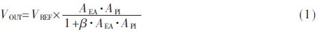
Among them, AEA is the closed loop gain of the error amplifier, API is the closed loop gain of P1 of the power tube, β is 
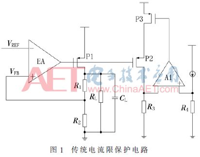
The working principle of the current limiting protection is that the sampling tube P2 mirrors the current of the power transistor P1 in proportion to the equation (2).
The mirror current IP2 is converted into the opposite terminal V1 of the voltage comparator A1 through the resistor R3, and compared with the fixed voltage V2 to control the switch P3 to be turned on or off, thereby controlling the gate voltage of the power transistor P1. When the current IP1 flowing through the power tube is small, V1
2 programmable current limit protection circuit proposed in this paper
Aiming at the shortcomings of traditional current-limiting protection circuit such as inaccurate current sampling and unacceptable current limit threshold, this paper designs a programmable current limit protection circuit based on the traditional current-limiting protection circuit structure. The designed maximum load capacity of the LDO is 3 A. The current limit circuit can accurately sample the power tube and adjust the current limit (0.2 A~4.5) by changing the off-chip resistance (8 kΩ~70 kΩ). A) The specific circuit is shown in Figure 2.

The sampling tube P0 mirrors the output current of the P1 tube of the power tube according to the size ratio of the MOS tube and obtains the formula (3):

P4~P6 tubes and M1~M4 tubes are series structure current mirrors. The function of the series PMOS tubes is to reduce the complexity in the layout production process and to weaken the effect of the channel length modulation of the tubes. The effect is to reduce the L value of the MOS tube by increasing the L value. The small channel length modulation factor [7] achieves high PSRR. At the same time, instead of the traditional structure of the voltage comparator, the two currents are directly compared to realize the control of the drain end of the P2 tube, that is, the gate voltage of the power transistor.
When ICS is greater than IPCL, the M3 and M4 tubes operate in the linear region, the voltage at point A is less than VTHN, and the P2 tube is turned on so that the gate voltage of the power transistor is clamped to VCC, and the power transistor is forcibly turned off and the output current becomes smaller. Played the role of current limiting protection [8]; When IPCL is greater than ICS, P3 and P4 tube work in the linear zone, point A voltage is greater than VCC-|VTHP|, P2 tube is in the cut-off state, LDO normal work.
Among them, the resistance RPCL is the external resistance of the chip of the programmable current limit, change the value of the electric current limit through the peripheral size, its range is 8 kΩ- 160 kΩ. VREF is the 0.6 V voltage generated by the internal reference voltage, VOUT is the output voltage of LDO, VFB is the feedback voltage of LDO, P0 is the adjustment tube of LDO, and P1 is the sampling tube with the ratio of width to length of P0 tube 1:54 000. This ratio, which is the CSR in formula (3), is 5 400.
The non-inverting terminal of the operational amplifier AMP1 is the drain of the sampling transistor P1 and the output terminal VOUT of the LDO is the inverting terminal. According to the principle of the “virtual short-term virtual-break†of the operational amplifier, the drain voltage of the P1 tube is clamped to the VOUT voltage, making the P1 tube. The three-terminal voltage is exactly the same as the three-terminal voltage of the power transistor P0 [9] in order to obtain a precise mirror sampling current and to achieve a sampling of 1/54 000 of the adjustment tube current.
In the same principle, the voltage of the port PCL is equal to the value of the feedback voltage VFB through the operational amplifier AMP2. Under the fixed voltage, the current limit can be set by changing the size of the external resistor RPCL. Equation (4):
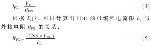
Among them, in this paper VREF = 0.6 V, CSR is the current sampling ratio, this article is 56 000.
When the LDO is operated under a large input-output voltage difference, if the current limiting current is large, it is easy to damage the chip because the power consumption is too large. At this time, the resistor RPCL should be increased to prevent the LDO from operating and burning the chip under a large power consumption. When the LDO operates at a small input-output differential voltage, the RPCL should be reduced to increase the current limit threshold, so as to avoid mis-operation of current-limit protection under large load current conditions [10]. Through the programmable design of the current limit, the normal operation of the circuit under different input-output configurations can be satisfied.
3 simulation results
According to the above theoretical analysis and description of the design process, a programmable current limit circuit for LDO is designed. The following is based on the TSMC 0.25 μm BCD process, the circuit designed in this paper is combined and simulated. The theoretical inference of this paper is verified by configuring the input voltage, output voltage and off-chip resistance RPCL.
With the same input voltage (5.5 V) and the same output voltage (1.8 V), the load change transient simulation is performed by setting different RPCL resistance values ​​to observe the change of the programmable current limit. The simulation curve is shown in the figure. 3 shows.
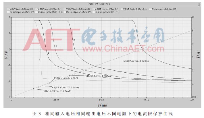
In the simulation graph 3, the off-chip resistance RPCL of curve 1 is 10 kΩ, the programmable current limit is 3.38 A; the curve 2 off-chip resistance RPCL is 22.5 kΩ, the programmable current limit is 1.6 A; the curve 3 external resistors RPCL is 35 kΩ, the programmable current limit is 1.06 A; the curve 4 external resistor RPCL is 47.5 kΩ, the programmable current limit is 758.6 mA; the curve 5 external resistor RPCL is 60 kΩ, and the programmable current limit is 616.7 mA. Achieving a programmable design with different off-chip resistors RPCL at the same output current limit.
In the same input voltage (5.5 V), the same RPCL resistance (10 kΩ), through the setting of different output voltages, the transient simulation of the load changes, observe the changes in the programmable current limit, the simulation curve shown in Figure 4 As shown.
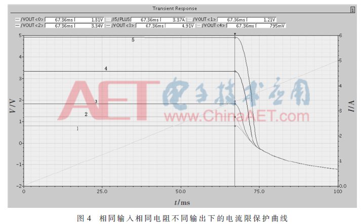
In the simulation graph 4, the input voltage is 5.5 V, the off-chip resistance RPCL is 10 kΩ, and the current limit curves at 0.8 V, 1.2 V, 1.8 V, 3.3 V, and 4.9 V, respectively, can be seen. With different output configurations, the current limit is approximately 3.4 A. This is in accordance with the design principle. The same programmable current limit is used for the same RPCL.
With the same output voltage (1.8 V) and the same RPCL resistance (10 kΩ), the load transient simulation is performed by setting different input voltages to observe changes in the programmable current limit. The simulation curve is shown in Figure 5. As shown.
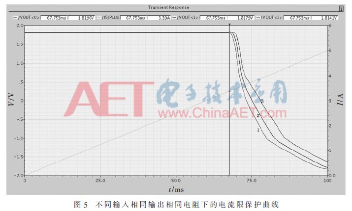
Different input voltages are set for the same RPCL resistance value (10 kΩ). The input voltage of curve 1 is 5.0 V, the input voltage of curve 2 is 3.3 V, and the input voltage of curve 3 is 2.2 V. It can be seen that the programmable current limit is about 3.4 A under the condition that different input voltages and RPCL are kept at a fixed value, which conforms to the design principle.
In the case of an input voltage of 5.0 V and an output voltage of 1.8 V, a simulation test is performed by adjusting the size of the programmable current limit resistor RPCL to obtain the correspondence between the programmable current limit and the resistance RPCL, as shown in FIG. 6 .

The RPCL in the fitting curve is brought into the equation (5), and the theoretical results and the simulation results in FIG. 6 are within 10%, and the current limit can be programmed better.
In the case of an input voltage of 2.5 V and an output voltage of 1.8 V, the output voltage changes with load as shown in Figure 7.

The simulation curve is shown in Fig. 7. The LDO designed in this paper is simulated under the TT process corner. The simulation results show that the load current varies within the range of 0~3 A, and the LDO can be normally output, and the change of VOUT is only 70. About μV.
4 Conclusion
Based on the 0.25 μm BCD process of TSMC, a programmable current limit circuit for LDO is designed in this paper, which effectively avoids the disadvantage of the traditional current limit circuit in which the current limit value is not adjustable. The current limit in this paper can be adjusted by configuring the size of the external resistor RPCL. Within the range of 2 V~5.5 V input voltage and 1.2 V~5 V output voltage, the maximum load capacity of 3 A is realized, and the programmable current limit can be adjusted within the range of 0.2 A~4.5 A. Simulation results show that the current limit circuit designed in this paper achieves the programmable current limit threshold and meets the design requirements.
Tobacco control has been a common global concern, while the traditional tobacco industry gradually, new tobacco has become the new strategic layout of tobacco giants. In this context, the emergence of e-cigarettes has further led to the replacement of traditional tobacco. At present, there are already a thousand different types of e-cigarettes, which have undergone several stages of development. The e-cigarette we are introducing today is the CBD pod systewm, a new type of e-cigarette. In this article we will combine the characteristics of the CBD with a brief analysis of it.
·Anti-anxiety
According to scientific studies,CBD can help depressed patients reduce their anxiety. The use of CBD can help maintain endogenous cannabinoids at a reasonable level, making the patient feel good and happy physically, and without any dependence.
·Anti-ageing
CBD is very powerful in anti-ageing. As a non-psychoactive component of the cannabis plant CBD inhibits the glutamate toxic response of cortical neurons and suppresses excessive oxidative stress, helping the body to achieve anti-ageing effects.
·Anti-inflammatory
CBD reduces the free radicals that cause neurodegenerative diseases and reduces swelling through its anti-inflammatory effects. In addition, CBD stimulates appetite and relieves pain.
China Disposble Vape Pen,E-Cigarette Cbd Vaporizer,Best Disposable Cbd Vape Pen,Disposable Cbd Vape
Shenzhen MASON VAP Technology Co., Ltd. , https://www.e-cigarettefactory.com