As a universal standard device functional test interface, JTAG is flexible, efficient and easy to implement. It is an important external interface for microcontrollers, microprocessors, DSPs, SoCs and other devices. It can not only be used to test internal function module status, but also to implement in-circuit debugging (ICE) function. It is through the JTAG interface that the ARM family of processors use the internally integrated ICE functionality and use this approach for in-circuit debugging. In addition, devices such as CPLDs and FPGAs can all be programmed or downloaded online using the JTAG interface. Therefore, the JTAG interface has become an essential interface for complex chip systems and plays an important role in chip testing, debugging, and implementation of other special functions.
Fundamental
The JTAG standard is the IEEE 1149.1 standard. Joint Test Action Group JTAG (Joint Test Action Group) drafted the Boundary Scan Testing (BST) specification, which specifies a test access port (TAP) and boundary scan structure for digital integrated circuits, and solves the problem of digital circuit height. Some testing problems brought about by integration. It also provides a method of accessing and controlling the on-chip emulation (ICE) module. The ICE module generally includes internal scan and self-test functions that can well support the development of integrated circuits.
How does the JTAG standard work?
The basic idea of ​​boundary scan technology is to add a shift register unit near the input and output pins of the chip. Through these boundary scan register units, the input and output signals of the chip can be observed and controlled. In addition, the boundary scan (shift) register units near the chip input/output pins may be connected to each other to form a boundary-scan chain around the chip. The general chip will provide several independent boundary scan chains for complete test functions.
In the JTAG standard, registers are divided into two major categories: DR-DATA Registers and IR- Instruction Registers. The Boundary Scan Chain Register is a very important data register. Boundary scan chains can be used to Observe and control the input and output of the chip. The instruction register is used to control the data register. The TAP is a general-purpose port. All data registers and instruction registers provided by the chip can be accessed through the TAP. Control of the entire TAP is performed through the TAP controller. The TAP includes five signal interfaces: (1) TCK (Test Clock), which provides an independent basic clock signal for TAP operation. (2) TMS (Test-Mode Selector), used to control the conversion of the TAP state machine. (3) TDI (TestData Input), a serial input for JTAG instructions and data. The rising edge of TCK is sampled and the result is sent to the JTAG register. (4) TDO (Test Data Output), a serial output of JTAG instructions and data. It is output to TDO on the falling edge of TCK. (5) TRST, is the reset input signal of the JTAG circuit, active low.
Through the state transition of the TAP controller, access to the data register and the instruction register can be realized, thereby realizing the control of the JTAG test circuit. The TAP controller has a total of 16 states, as shown in Figure 1. TMS and clock TCK can be selected through test mode to control the transition of state.
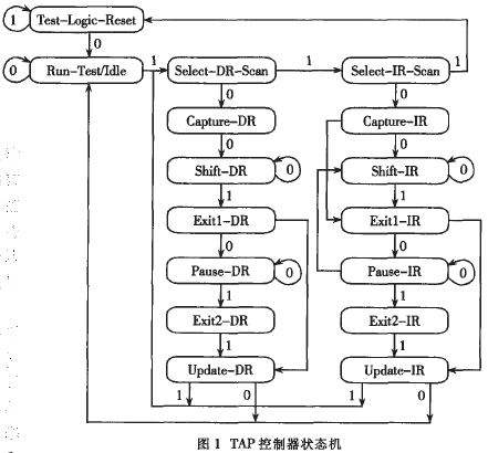
The instruction register allows specific instructions to be loaded into the instruction register to select the test to be executed or to select the test data register to be accessed. Each chip that supports JTAG debugging must contain an instruction register. The JTAG standard requires that the basic instructions supported by the chip include: EXTEST, INTEST, SAMPLE/PRELOAD, BYPASS, HIGHZ, and so on.
ARM7TDMI debugging principle
From a functional point of view, the ARM7TDMI processor mainly includes three major parts:
(1) ARM CPU Main Processor Logic , including hardware support for debugging;
(2) Embedded ICE-RT Logic, including a set of registers and comparators, used to generate debug exceptions, set breakpoints, and watchpoints;
(3) TAP controller, which controls and operates the scan chain through the JTAG interface.
The ARM7TDMI provides four scan chains, namely scan chains 0, 1, 2 and 3. The peripheral circuitry of the ARM7TDMI core, including the data bus, can be accessed through scan chain 0. The length of the scan chain is 113 bits, including 0 to 31 bits of the data bus, core control signals, 0 to 31 bits of the address bus, and control signals of the embedded ICE-RT. The scan chain 1 is a subset of the scan chain 0 and has a length of 33 bits, and specifically includes 0 to 31 bits of the data bus and the BREAKPT signal. The scan chain 1 is much shorter than the scan chain 0, and the scan chain 1 can be faster. Insert instructions or data inside the ARM7TDMI. The length of the scan chain 2 is 38 bits. This scan chain is used to access the internal registers of the embedded ICE-RT. By accessing the internal registers of the embedded ICERT, the ARM7TDMI can be brought into debug state, set breakpoints, and set observation points. By scanning chain 3, the ARM7TDMI can access the outer boundary scan chain, which is rarely used.
The debugging status and normal operation status of the ARM7TDMI are different. In normal operation, the ARM7TDMI is driven by the MCLK (MemoryClock) and operates normally. In the debug state, the normal operation of the ARM7TDMI is interrupted and isolated from the rest of the system. You can read and write the ARM7TDMI internal registers and modify the contents of the memory by inserting specific ARM/THUMB instructions through the scan chain. After completing the required operations, you can use the RESTART JTAG instruction to return the ARM7TDMI to normal operation and restore the original operation.
Embedded System Implementation of JTAG Debugger
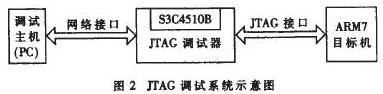
The JTAG debugger hardware is implemented on an ARM7-based embedded system. The system uses an ARM chip S3C4510B with an Ethernet interface as the core processor and μClinux as an embedded operating system. The JTAG debugger software mainly includes two parts: the interface module of the JTAG debugger and the target machine and the interface module of the debug host. The specific block diagram shown in Figure 2.
Embedded System Design
Design and build standard S3C4510B application system, mainly configured as 2MBFLASH, 16MB SDRAM, 10/100Mbps adaptive Ethernet port, terminal interface, parallel I/O interface and so on. Using the S3C4510B general-purpose I/O port, P[4], P[5], P[6], and P[8] simulate the four signal interfaces of the TAP in the JTAG standard, namely TCK, TMS, TDI, and TDO.
From the software point of view, the μClinux operating system needs to be ported to the S3C4510B-based JTAG debugger hardware platform designed for the development of network-based debugger software. μCLinux is an embedded operating system designed for processors without a memory management unit (MMU). It inherits the powerful network functions of desktop Linux. Its kernel adopts a modular organization structure, and is increased by adding or removing kernel modules. Reduce the function of the system.
In general, JTAG timing can be simulated on a PC through parallel port, and the JTAG debugger can also be designed according to a standard emulator. Different from the above solutions, this design uses open source software to design the JTAG debugger application software. The main reference is the software jtager - 1.0.0 developed by the Open-JTAG team to realize the JTAG operation through the PC parallel port, and the parallel port of the PC is used. The operation is changed to the operation of the S3C4510B interface. By setting the value of the general I/O port mode register IOPMOD of S3C4510B, P[4], P[5], P[6] can be set as the output mode, and P[8]. Set to input mode, and then set the I/O port data register IOPDATA by programming to control the states of P[4], P[5], P[6], P[8] to achieve the timing required by the JTAG standard. Subsequently, according to the ARM7TDMI debugging features, modify the operating code and increase the remote debugging capabilities through the network.
ARM7TDMI JTAG Instruction Implementation
The ARM7TDMI has an instruction register length of 4 bits and can be loaded into the instruction register through the TAP and JTAG interfaces. In the CAPTURE-IR state, the fixed value B0001 is always loaded into the instruction register. In the SHIFT-IR state, new instructions supported by the ARM7TDMI can be serially input from the TDI while the fixed value B0001 is serially output from the TDO. By outputting this fixed value, it can be judged whether the current operation is correct. In the UPDATE-IR state, the newly entered instruction is loaded into the instruction register. After returning to the RUN-TEST/IDLE state, the new instruction takes effect immediately.
IDCODE and SCAN_N are commonly used JTAG commands in ARM7TDMI debugging. The binary code for the IDCODE command is 1110. The IDCODE command connects the DevICe Identification Code Register to TDI and TDO. The length of the Device Identification Code register is 32 bits, and the ID of the ARM7TDMI can be read through the TAP. The binary code of the SCAN_N command is 0010. The ARM7TDMI provides four scan chains. The scan chain that needs to be accessed can be selected through the SCAN_N instruction. The process of selecting the scan chain is: first load the SCAN_N instruction into the instruction register, which will connect the 4-bit scan chain selection register to the TDI and TDO; the transfer of the TAP state will enable the selected scan chain. Connected between TDI and TDO.
In addition, implementations of JTAG instructions such as BYPASS, INTEST, and RESTART are similar to the implementation of the above two instructions.
Embedded ICE-RT logic implementation
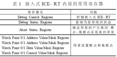
The embedded ICE-RT is an online simulation function module integrated within the ARM processor. It interacts with the outside world through the JTAG debugging interface. The commonly used registers included in this table are shown in Table 1.
To access the registers inside the embedded ICE-RT, access the Debug Control Register through scan chain 2. Implementation: Write the SCAN_N instruction to the JTAG instruction register through the TAP, and write the value 2 to the scan chain select register via TDI. Select scan chain 2 before accessing any embedded ICE-RT internal register through scan chain 2. The INTEST instruction is also required to set the scan chain currently selected by the SCAN_N instruction to the internal test state. The process of writing the INTEST instruction is similar to the process of writing the SCAN_N instruction. Next, you can access the embedded ICE-RT internal registers through scan chain 2 to implement the basic debug function of the ARM7TDMI.
Realization of ARM7TDMI register and memory access
The boundary scan chain is distributed around the 32-bit data bus of the ARM7TDMI. The ARM7TDMI must perform a 32-bit data bus for each instruction fetch or data storage. In this way, through the boundary scan chain 1, new instructions or new data can be inserted, and data appearing on the data bus can also be captured. In this way, the general registers and system memory of the ARM7TDMI can be checked and modified.
Taking the value of the read register R0 as an example, the operation of the boundary scan chain 1 is described, as shown in FIG. 3 .
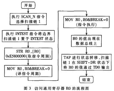
The value of the read register R0 can be implemented with the instruction STR R0, [R0] (machine code 0xE5800000). This instruction stores the value of register R0 into memory location R0. Since the ARM7TDMI is isolated from the external when the ARM7TDMI is in the debug state, the instruction cannot actually access the memory cell and does not have any effect on the memory cell. Using the instruction STR R0, [R0] causes the value of register R0 to appear on the data bus so that it can be captured by scan chain 1 and then output from TDO. The execution of the instruction STR R0, [R0] requires two instruction execution cycles. In the first instruction execution cycle, address calculation is performed. In the second instruction execution cycle, the value of register R0 is placed on the data bus. The method of writing to ARM registers and accessing memory is similar to this. All of them are through scan chain 1, but the instructions used are different.
network programming
Through network programming, remote debugging of the target system can be achieved. Figure 4 is a flow chart of network communication between PC and emulator. Network communication is achieved through socket programming under μClinux. First, the PC (debug host) sends commands to the emulator through the network. The emulator analyzes the debugging commands through a unified program interface, and converts the debugging commands to the timing required by the JTAG standard. The /O line is sent to the target board; then the target executes the command and returns the debugging information obtained after the command is executed to the emulator. Then the emulator sends the debugging information to the PC through the network so that the user is debugged on the PC. information.
JTAG debugger test and partial execution results
This design finally completed a JTAG debugger operating under the Linux terminal. After the debugger is powered on, the debugger client program is automatically run under μClinux. At the same time, the JTAG debugger server-side program jtager is run in the PC's Cygwin environment to establish a network connection. Then type the user debug command under Cygwin and do the following:
(1) Write CPU status on the target board;
(2) Read and write external device registers that are addressed in a unified memory space;
(3) Read and write RAM on the target machine;
(4) Read and write target solid-state storage devices, such as Flash;
(5) Debug the embedded ICE-RT.
There are many user commands designed to implement the debugger. The following only lists the results of executing the two typical commands IDCODE and REG.
After executing the IDCODE command, a CPU ID number in the target development board based on S3C4510B is read out to obtain Device ID="0x1F0F0F0F". By analyzing the timing relationship of several JTAG interface signals through a logic analyzer, it is possible to observe the access process of the JTAG scan connection and the transition of various states in the process, and the result is consistent with the JTAG_debugging principle.
After executing the RE command, the contents of the registers R0 to R15 and the contents of the CPSR are obtained, that is, all register values ​​of the target development board processor S3C4510B in the current processor mode are read out, and they can also be modified by other commands.
In addition, 17 internal debug registers with different widths of the embedded ICE-RT can be accessed through the scan chain 2, and the three ways in which the target ARM7TDMI enters into the debug state through these registers, that is, control of the DBGRQ signal, breakpoint, and observation point, are realized. Online debugging function.
The JTAG debugger implemented in this paper has basic debugging functions. It does not have a complete user interface, especially the graphical user interface. In addition, the network function also needs to be further improved. However, the design and implementation of debuggers are valuable for designing similar debuggers. To increase the JTAG debugger rate, JTAG timing can also be implemented using a CPLD or FPGA, interfaced with the debugger CPU via memory, which will increase the speed and reduce the burden on the debugger CPU.
LED street lights achieve ultra brightness/luminance; energy-saving over 70%. Special modular design for theLens (independent modules) and high luminous efficacy, high CRI, easy for maintenance.Intelligent and isolated power supply (NS semiconductor and Japan Rubycon capacitor), reliable and stable; automatically reduce current against overheating working temperature
Led Street Light,Street Lamp,Led Lamp,Street Lamp Post
Yangzhou Beyond Solar Energy Co.,Ltd. , https://www.ckbsolar.com