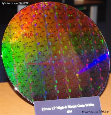
 At the Common Platform 2011 Technology Conference held last week, the IBM-led General Technology Alliance each introduced the latest developments in its semiconductor manufacturing process, and the Blue Giant itself even took out the world's first 20nm process wafer.
 According to reports, this wafer not only uses the industry-leading 20nm LP HKMG (low-power high-k metal gate) manufacturing process, but also introduces Gate-Last technology, which is simply to perform the drain/source region on the silicon wafer. The metal gate is formed after the ion implantation operation and the subsequent high temperature annealing step are completed.
Gate-Last (gate) and Gate-First (gate) are two major technical schools that implement the HKMG structure transistor. The main difference is that the drain/source region of the silicon is ion-implanted, the high-temperature annealing, and the formation of the metal gate are successively. . Intel insisted on using Gate-Last from the 45nm process, and TSMC also decided to start with 28nm. The IBM Alliance has always supported Gate-First, including the 32/28nm process, and it now appears that 20nm will be its first inflection point.
IBM did not disclose what kind of products this wafer will be used for, but since it is a low-power version, it should not be used on high-performance chips such as CPUs and GPUs.