0 Preface
As an optical instrument, the integrating sphere has been widely used in related fields such as photometry and radiosmetry for nearly a hundred years. In many research applications, integrating spheres are often used as uniform radiation sources to test focal plane array optoelectronic devices such as CCD or CMOS. However, due to the influence of various factors such as the integral spherical shell processing, the internal screen position, the actual thickness of the diffuse coating, and the geometric position of the internal light source during the actual manufacturing and installation process, the actual integrating sphere radiation source opening Illumination uniformity is not ideal. On the other hand, scientific-grade CCDs used in aerospace, astronomy and other fields often need to work at lower temperatures. If the device is tested at the integrating sphere, the heating problem of the internal light source of the integrating sphere can have a negligible effect on the device. Therefore, it is not appropriate to perform the test of the photovoltaic device at the exit of the integrating sphere light source according to the ideal situation. In view of this misunderstanding, this paper focuses on the uniformity of the illumination distribution on the light-receiving surface of the optoelectronic device at different distances from the integrating sphere radiation source. Based on theoretical analysis and experimental tests, the illuminance on the receiving surface of the optoelectronic device at different distances from the integrating sphere radiation source is obtained. The law of uniformity distribution.
1 theoretical analysis
As shown in Fig. 1, when testing an imaging photoelectric system such as a space remote sensing camera, an integrating sphere radiation source is required to provide a uniform (radius) luminance field to fill the optical system of the system under test and image on the focal plane array optoelectronic device. The device response signals are collected into a computer for recording and sorting.
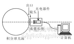
Figure 1 Schematic diagram of imaging photoelectric system test
When testing CCD and other focal plane array optoelectronic devices, as shown in Figure 2, the integrating sphere radiation source is required to provide a uniform (radius) illumination field to cover the light-receiving surface of the optoelectronic device. This test requires careful consideration of the illumination on the light-receiving surface of the optoelectronic device. Distribution.
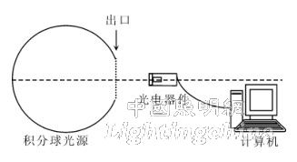
Figure 2 Photoelectric device test schematic
2.1 ideal integrating sphere radiation source
Assuming that the integrating sphere radiation source is an ideal Lambertian body, that is, the integral sphere exit radiance B is evenly distributed, there is a relationship:
As shown in Fig. 3, the integrating sphere exit surface O is parallel to the optoelectronic device receiving surface O', M is any point on the plane O, and N is any point on the plane O', then the point D is the micro-element dN to the M-point micro-element dM Angular coefficient is
In the middle  The distance between the M point and the N point;
  versus
  Two-point axis and
  Angle of inclusion; dM is the micro area of ​​M point. The illuminance response generated by the light radiated from M at N can be expressed as
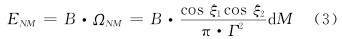
Figure 3 Numerical analysis model of the integrating sphere radiation source
From the geometric relationship in Figure 3:
Where: L is the line connecting point O and point O', that is, the distance between the light receiving surface of the photoelectric device and the exit surface of the integrating sphere; α is the angle between OM and O'N; R is the length of OM; r is O'N length. Substituting equations (4) and (5) into equation (3) gives:
(6) represents the illuminance response generated by a radiation micro-element on the exit plane O of the integrating sphere radiation source at a distance O' above the plane O'. If the radiation micro-element is integrated in the entire exit plane O, then The illuminance response EN of the integrating sphere radiation source at N can be obtained as
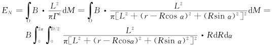
Where: D = 2R is the diameter of the integrating sphere outlet; d = 2r is the diameter of the receiving surface of the photovoltaic device.
Definition: The uniformity of illumination on the light-receiving surface of the optoelectronic device at a certain distance from the integrating sphere radiation source. The ratio of the illuminance Ee at the far axis of the receiving surface to the illuminance Eo at the center:
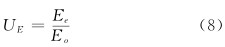
According to the numerical calculation of (8), the uniformity of the illumination surface illumination of the photoelectric device at different distances from the outlet of the integrating sphere is obtained, as shown in Fig. 4.
Figure 4 Uniformity distribution of illuminance of ideal integrating sphere radiation source
2.2 ideal integrating sphere radiation source
The premise of the numerical analysis method is to assume that the integrating sphere radiation source is an ideal Lambertian body, and under actual conditions, the integrating sphere radiation source is a non-ideal Lambertian body. For the illuminance distribution of the integrating sphere radiation source under non-ideal conditions, we use the Monte Carlo-based ray tracing method to simulate an integrated sphere radiation source model with 94% uniformity of the exit radiance surface. The simulation model of the non-ideal integrating sphere radiation source shown in Fig. 5 is established with reference to the integrating sphere analytical model of Fig. 3. The simulation model was experimentally analyzed using 3.2×10⁷ rays in the optical software TrancePro. The simulation results of the non-ideal integrating sphere radiation source are shown in Fig. 6.
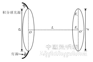
Figure 5 Simulation model of non-ideal integrating sphere radiation source
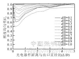
Fig. 6 Simulation results of illuminance uniformity of non-ideal integrating sphere radiation source
It can be seen from Fig. 4 and Fig. 6 that: 1) the illuminance uniformity of the non-ideal integrating sphere exit plane is poor. When the diameter of the receiving surface of the optoelectronic device is equal to the diameter of the integrating sphere exit (d/D=1.0), the uniformity of illumination is only 83. %, not 100% under ideal conditions; 2) When the photoelectric device is closer to the integrating sphere exit (L/D<0.5), the uniformity of illumination on the light receiving surface is worse than that at the exit, and the larger the diameter of the light receiving surface, the more uniform the illumination 3) As the distance between the optoelectronic device and the integrating sphere exit increases, the illuminance uniformity undergoes a process of first becoming worse and then getting better. When the optoelectronic device is far enough away from the radiation source (L/D ≥ 3), the illumination is uniform. Sex is better than the exit.
3 experiments and discussion
3.1 Illumination uniformity experiment
Two sets of integrating sphere radiation sources, DIS70 and DIS180, were tested separately. The integrating sphere diameter, outlet diameter, aperture ratio and radiance plane uniformity parameters are shown in Fig. 1.
The illuminance uniformity test scheme of the integrating sphere radiation source is: the illuminance detector is fixed on the two-dimensional translation stage, and after selecting the distance L between the translation plane of the translation stage and the exit plane of the integrating sphere, the detectors are arranged at appropriate intervals in the scanning plane of the translation stage. Grid scan. Using this test scheme, the integrated sphere radiation sources DIS70 and DIS180 were tested experimentally. The data were sorted and listed in Tables 2 and 3. D is the diameter of the integrating sphere exit and d is the diameter of the receiving surface of the optoelectronic device.
Table 1 Integral sphere radiation source DIS70 and DIS180 parameters
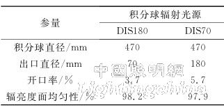
Table 2 DIS70 Illumination Uniformity Test Results

Table 3 DIS180 Illumination Uniformity Test Results
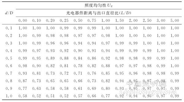
Analysis of Table 2 and Table 3 data shows that: 1) For the actual integrating sphere radiation source, the illumination uniformity of the exit plane is not 100% under ideal conditions, and the worst is only 58% (d/D=1.0); 2) When the photoelectric device is closer to the integrating sphere exit (L/D<0.5), the uniformity of illumination on the light receiving surface is worse than that at the exit. The larger the diameter of the light receiving surface, the worse the uniformity of illumination. The worst value is 51% (L/D). =0.2,d/D=1); 3) When the photoelectric device is far enough away from the integrating sphere light source (L/D≥3), the uniformity of illumination on the light receiving surface is better from the difference; if d/D≤0.5, the illumination is The uniformity can be better than 99%. Although the two sets of integrating sphere light sources have high radiance surface uniformity, which can meet the calibration test requirements of the imaging optoelectronic system, if it is directly used to test optoelectronic devices such as CCD without careful consideration of the device test position, the optoelectronic device will be Test accuracy has a large impact.
3.2 illuminance uniformity distribution law
Fig. 7 shows the uniformity distribution of illuminance when the diameter of the light-receiving surface of the photovoltaic device is directly equal to the outlet of the integrating sphere (d/D = 1.0).
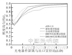
Figure 7 illuminance uniformity distribution law
It can be seen from Fig. 7 that with the increase of the distance between the optoelectronic device and the integrating sphere light source, the four curves all appear to decrease to the minimum value and then rise again. According to this phenomenon, the uniformity of the illumination surface illumination of the photoelectric device can be summarized under the actual conditions. Distribution:
1) The uniformity of the plane illumination of the integrating sphere radiation source is very poor, not 100% under ideal conditions, and it is not suitable for the test of optoelectronic devices at the exit;
2) When the photoelectric device is far enough away from the radiation source (3 ≤ L / D ≤ 5), the illuminance uniformity of the light receiving surface is better than 97%, and the photoelectric sensor can be tested in the distance using the integrating sphere radiation source.