1 Overview
The power MOSFET was originally developed from a MOS integrated circuit. It increases the withstand voltage of the device by increasing the lateral distance between the source and the drain, thereby achieving high-voltage driving in the integrated circuit. Power MOSFETs have been widely used in power electronics, consumer electronics, automotive electronics and hydroacoustic engineering. Although the power MOSFET has the advantages of high efficiency, simple structure, and convenient digital control, the power electronic device used has poor tolerance to overvoltage and overcurrent, and is easy to burn. Therefore, the design of the protection circuit is very important, and the response time is required to be protected. Do microseconds. Power MOSFET protection mainly refers to overcurrent protection, and for overvoltage conditions, absorption circuits are generally used for suppression.
In the design and use of underwater acoustic transmitter power MOSFETs, the power amplifier is often burned easily due to abnormalities in the input signal and environmental interference.
Aiming at the damage or burnout of the power MOSFET, a programmable protection circuit with CPLD (complex programmable logic device) as the core device is specially designed in the underwater acoustic transmitter application. Currently CPLD has been widely used. It has flexible architecture/logic unit, fast processing speed, high integration, large-scale circuit, flexible programming, short design and development cycle, low design and manufacturing cost, advanced development tools, standard products without testing, stable quality, and Real-time online inspection and wide application range, so it is gradually applied to various types of protection circuit design.
In view of the many advantages of CPLD, this design uses a separate CPLD chip as the core, and does not require a single-chip or DSP control to solve the serious problem caused by the abnormality or failure of the excitation signal of the high-power transmitter with MOSFET as the core. The safe and stable operation of the MOSFET circuit provides protection. The CPLD protection circuit can prevent the abnormal signal from entering the subsequent stage to damage the power MOSFET by simply changing the code parameters under the condition of inputting a high-level long pulse, continuous signal and short-cycle pulse, etc., to achieve protection of the circuit.
2. The basic principle of power MOSFET
The basic principle of the power MOSFET circuit is to form an H-bridge type D-type switching amplifier with four power-off devices V1, V2, V3 and V4 (as shown in Figure 1). In Figure 1, the diagonal power devices (V1 and V4, V2 and V3) are turned on and off simultaneously. Devices on the same side (V1 and V2, V3 and V4) are alternately turned on and off, and the excitation signals differ by 180. Thus, when the upper device is turned off (on), the lower side is turned on (turned off). Therefore, the potentials at the two points A and B are switched according to the frequency (or pulse width) set by the input excitation signal, and are alternately switched between "+" and "-" of the power supply.
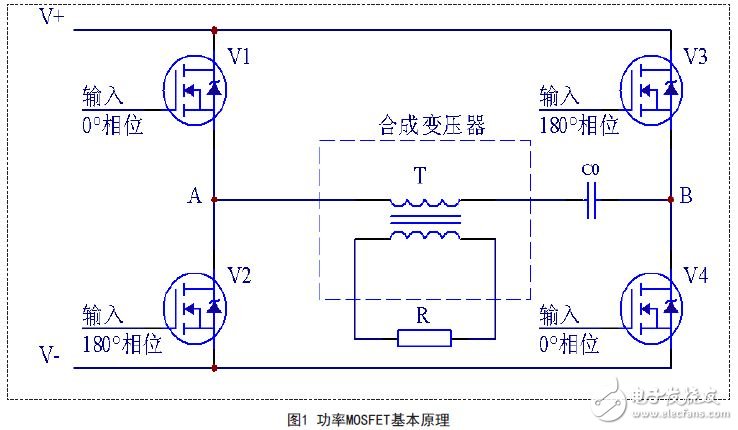
In the actual application process, there are high voltage and large current on the circuit, and the distributed capacitance and distributed inductance on the loop are very large. If the power device gate excitation signal is slightly faulty, it will cause overvoltage on the power loop (or Overcurrent) burns the device or device. Therefore, this power amplifier not only needs to have a complete overvoltage and overcurrent protection function, but more importantly, it requires the power device gate excitation signal input to the power amplifier bridge to be stable and reliable [4].
3. Protection circuit CPLD implementation
The internals of the CPLD protection circuit are mainly composed of power conversion, crystal oscillator, CPLD, and output port driver.
The block diagram of the protection circuit is shown in Figure 2.
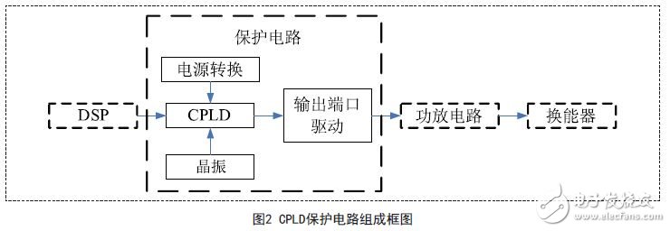
The core part of the protection circuit is mainly a CPLD, and all functions are realized by logic programming the device. In hardware, the analog output pulse from the DSP circuit is converted and protected, and the corresponding output is two driving signals and one envelope signal. The two output signals have the same envelope, time synchronization, and the signal is high and low. The envelope signal is the envelope of the two output signals, time synchronized. The two output signals are isolated and inverted by the optical isolation to provide a source of emission excitation signal for the power MOSFET, and the envelope signal provides a control signal for the power circuit after being separated by the optical isolation.
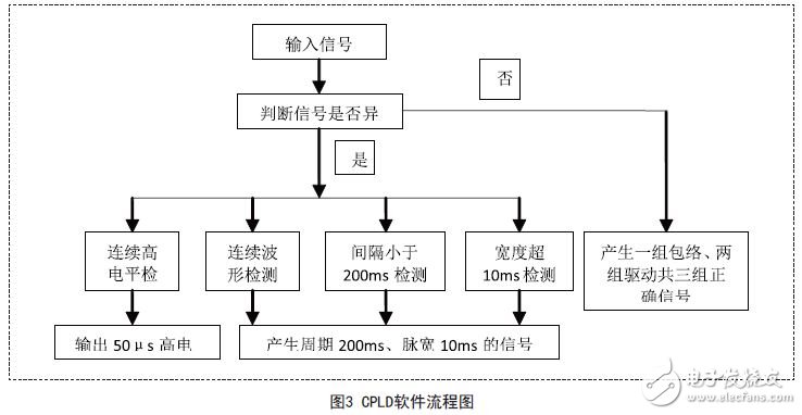
The CPLD protection circuit mainly inputs and protects the typical abnormal signals of the input MOSFET circuit, including the continuous wave signal, the short cycle pulse signal and the high level long pulse signal. All abnormal input signals are usually composed of these three signals. It is assumed that the continuous wave signal is a signal having a pulse width exceeding 10 ms; the short cycle pulse signal is a signal having a pulse period of less than 200 ms. The processing of other different parameter anomaly signals can be changed by simply setting the software counter. The protection circuit software flow chart is shown in Figure 3.
The specific protection functions and timing diagrams of the protection circuit are as follows:
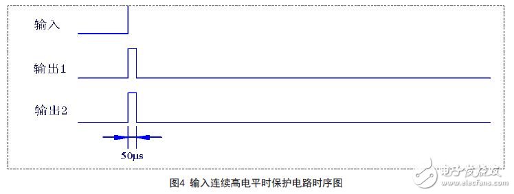
When the DSP circuit inputs a continuous high level to the protection circuit, the protection circuit starts to detect the first period of the 10 kHz frequency signal (ie, 100 μs) based on the first rising edge. If there is no lower edge, the protection output is 50 μs long. After the level, the output port is turned off and kept low. The two-way drive signal output and input timing are shown in Figure 4.
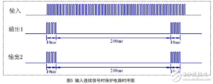
If the DSP circuit inputs a continuous waveform signal to the protection circuit, the protection circuit will use the first rising edge as a reference to output a 10ms pulse wave every 200ms to avoid continuous operation damage to the power MOSFET, two-way drive signal output and input signal timing. As shown in Figure 5.
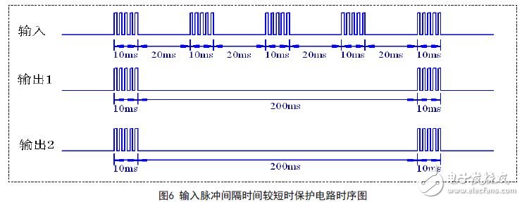
If the interval between the two pulses of the input signal is less than 200ms, the protection module will control the time of 200ms after the first pulse input, and keep returning to normal after continuing low level within 200ms, in response to the arrival of the next pulse signal, The pulse signal has a period of 20 ms as an example. The two-way drive signal output and input timing are shown in Figure 6.
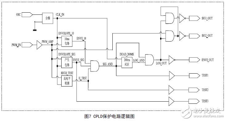
The logic diagram of the CPLD protection circuit implementation is shown in Figure 7.
The high energy from short wavelength UVC light is absorbed in the cellular RNA and DNA, damaging nucleic acids and preventing microorganisms from infecting and reproducing.
This absorption of UVC energy forms new bonds between nucleotides, creating double bonds or dimers." Dimerization of molecules, particularly thymine, is the most common type of damage incurred by UVC light in microorganisms.
Formation of thymine dimers in the DNA of bacteria and viruses prevents replication and ability to infect.
Disinfecting Light UV,Sterilization UV Lamp,Sterilization UV Disinfecting Light,Germicidal Tube Lamp with Base
Jilin Province Wanhe light Co.,Ltd , https://www.wanhelight.com