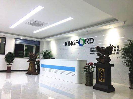
Shenzhen Kingford Co., Ltd  is an electronics manufacturing service provider and printed circuit board manufacturer, offers custom-designed electronics manufacturing and MID-sized OEMs and ODMs. A wide range of end markets that include PCBAs for Automotive, Communications, Computing, Consumer, Industrial, and Healthcare All these PCBAs are being exported to foreign markets, mainly to eastern Europe market. SHTL is dedicated to being a long-term PCBAs partner with our customers to achieve quality and cost optimization. Â
Â
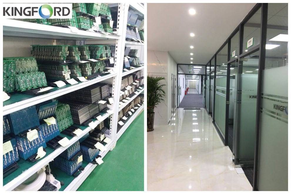
A professional PCB& PCBA design, product, sale manufacturer, established in 2010. Specially dedicate to Security, Industrial Automation, Medical, Household Appliance PCBA and Electrics products finished assembly. Currently with 100 workforce and covering 2, 000 square meters area, our products exported worldwide including North American, &Â South American, European Countries and Asia, etc.
PCB Technical standard:Â
Â
| Shenzhen kingford Technology Co.,LTD | ||
| Seq | Item | capability |
| 1 | Base Material | FR-4, High TG FR-4 , Halogen Free material ,CEM-3,CEM-1,PTFE,Rogers ,Arlon ,Taconic,Aluminum base,Teflon,PI ,etc |
| 2 | Layers | 1-40 ( ≥30 layers needs review ) |
| 3 | Finished inner/outer copper thickness | 0.5-6OZ |
| 4 | Finished board thickness | 0.2-7.0mm(≤0.2mm needs review),≤0.4mm for HASL |
| Board thickness≤1.0mm: +/-0.1mm 1 | ||
| 5 | Max panel size | ≤2sidesPCB: 600*1500mm Multilayer PCB: 500*1200mm |
| 6 | Min conductor line width/spacing | Inner layers: ≥3/3mil Outer layers: ≥3.5/3.5mil |
| 7 | Min hole size | Mechanical hole: 0.15mm Laser hole: 0.1mm |
| Drilling precision: first drilling      First drilling: 1mil                                                   Second drilling: 4mil | ||
| 8 | Warpage | Board thickness≤0.79mm: β≤1.0% 0.80≤Board thickness≤2.4mm: β≤0.7% Board thickness≥2.5mm: β≤0.5% |
| 9 | Controlled Impedance | +/- 5 % Ω(<50Ω),+/-10%(≥50Ω),≥50Ω+/-5% (needs review) |
| 10 | Aspect Ratio | 15:01 |
| 11 | Min welding ring | 4mil |
| 12 | Min solder mask bridge | ≥0.08mm |
| 13 | Plugging vias capability | 0.2-0.8mm |
| 14 | Hole tolerance | PTH: +/-3mil NPTH: +/-2mil |
| 15 | Outline profile | Rout/ V-cut/ Bridge/ Stamp hole |
| 16 | Solder mask color | Green,yellow,black,blue,red,white,matte green |
| 17 | Component mark color | white,yellow,black |
| 18 | Surface treatment | OSP: 0.2-0.5um HASL: 2-40um Lead free HASL: 2-40um ENIG: Au 1-10U'' ENEPIG: PB 2-5U''/ Au 1-8U'' Immersion Tin:0.8-1.5um Immersion silver: 0.1-1.2um Peelable blue mask Carbon ink Gold plating: Au 1-150U'' |
| 19 | E-Test | Flying probe tester : 0.4-6.0mm,max 19.6*23.5inch |
| Min spacing from test pad to board edge : 0.5 mm | ||
| Min conductive resistance :  5 Ω | ||
| Max insulation resistance : 250  MΩ | ||
| Max test voltage : 500 V | ||
| Min test pad diameter : 6 mil | ||
| Min test pad to pad spacing : 10 mil | ||
| Max test current  :  200 MA | ||
| 20 | AOI | Orbotech SK-75 AOI : 0.05-6.0mm,max 23.5*23.5inch |
| Orbotech Ves machine : Â 0.05-6.0mm,max 23.5*23.5inch | ||
PCB Manufacturing Capacity:
Base material:FR-4/CEM-1/CEM3/Ceramic/Teflon/Aluminum/Copper etc
PCBs: Rigid(0-22layers),Flexible(1-8layers),Rigid-flex(1-16layers,flex 8layers), MCPCB(aluminum and copper1-4layers)
Board thickness: 0.2mm--10mm
Copper thickness: 0.25 Oz -8 Oz
Max Panel Size: 1500 mm × 560 mm
Min. Hole Size: 0.075mm(3mil)
Min. Line Width/Spacing: 3mil
Surface Finishing: HASL/HAL, HASL Lead Free,ENIG,immersion silver,immersion tin,OSP,Plating Hard Gold,etc.
Solder Mask Color: White, Black, Yellow, Green, Red, etc.
Silkscreen Color: Black, White, Yellow, Red, Blue, etc.
Special Process: Buried hole, blind hole, Soldermask ink, Epoxy resin, Copper, Embedded Resistance, Embedded Capacity, Hybrid, Partial hybrid, Partial high density, Back drilling and impedance control.
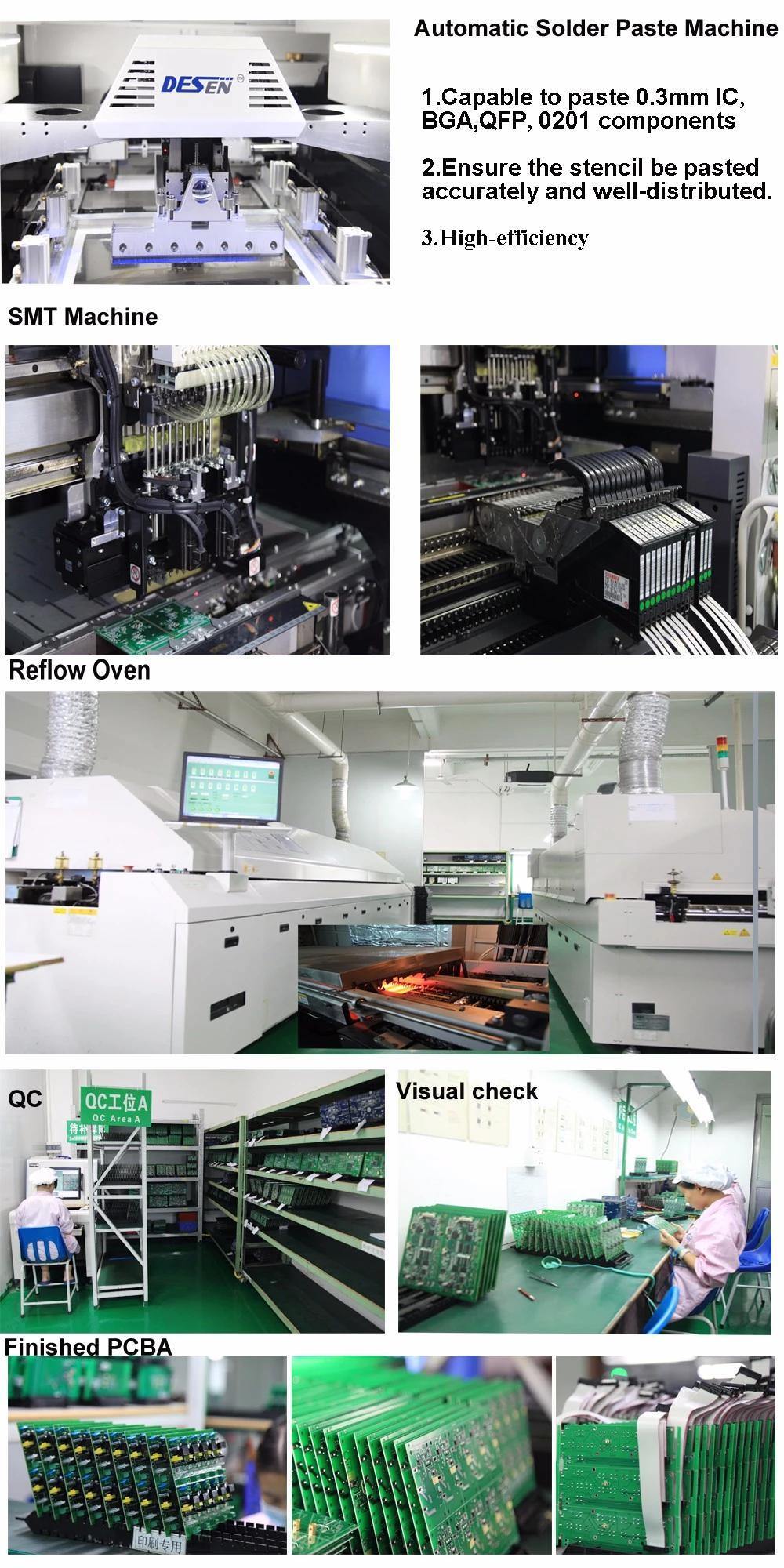
PCB Assembly Capacity:
SMT Capability:5KK points/Day,single-sided/double-sided,10 Lines
Reject rate of components: 0.3% (Capacitor and Resistance)No(IC)
Min. Package: 01005 chip /Â 0.35 Pitch BGA
Min. Precision: +/-0.04mm
Min. Precison of IC: +/-0.03mm
SMD Size:0201-150mm
Max. Height of components by machine:30mm
Min. Pin pitch of SMT: 0.2mm
Min. Ball pitch of SMT: 0.2mm
Min. Precision of Stencil: 5um
PCB Size of Assembly: 5x5mm-500*1500mm
PCB Thickness of Assembly: 0.1-10mm
BGA/μBGA: available;Solder paste/glue processing
DIP capacity: 0.30 million points per day
Max. Capability: Stable support for 200 products on production line at the same time
Functional testing&Casing assembly: upon customer's requirements
Full Range Of Testing Services:Â
â–ªAOI
â–ªFunction testing
â–ªIn circuit testing
â–ªX-ray for BGA testing
â–ª3D paste thickness test
â–ªFlash testing and earth bonding tests can also be undertaken where required
Using our X-ray machine, we test PCBs to component level and all wiring is fully inspected and tested
Advantages:
â–ªNo MOQ
â–ª18 years of PCB&PCBA turnkey services
â–ªQuick turn, Prototype, Low &Â medium &Â high volume
â–ªComponents sourcing,ODM&OEM services provide
▪ISO 9001-, ISO14001-,  ISO/TS16949, ISO13485, IATF16949, OHSAS18001certified,UL E352816
â–ª100% E-test,100% visual inspection, including IQC, IPQC, FQC and OQC
â–ª100% AOI inspection, including X-ray, 3D microscope and ICT
â–ªFast response within 24 hours,great pre-sales, sales, after-sales
â–ªAll kinds of Export/Import Processing Support,EX-Factory, FOB HK, FOB Shenzhen, FCA HK, FCA Shenzhen and DDU by express
â–ªAll kinds of payment:T/T,Paypal,WesternUnionÂ
â–ªGuarantee Sales Service,for all problems encountered kindly contact us, we will do the after service any time.
FAQ:
Q1:What service do you have?
We provide turnkey solution including PCB fabrication, SMT, plastic injection &Â metal, final assembly,testing and other value-added service.
Q2:What are the main products of your PCB/PCBA services?
Our PCB/PCBA services are mainly for the industries including Medical,Automotive,Communication.
Q3:Is IT a factory or trade company?
YES,we are a manufacturer with PCB factory located in China
Q4:Can we inspect quality during production?
 Yes, we are open and transparent on each production process with nothing to hide. We welcome customer inspect our production process and check in house.
Q5:How can we ensure our information should not let third party to see our design?
We are willing to sign NDA effect by customer side local law and promising to keep customers data in high confidential level.
Q6:What files required to get quotation from you?
 For PCB quotation, please provide the Gerber data/files and indication of related technical requirements as well as any special requirement if you have.
For PCBA quotation, please provide Gerber data/ files and also BOM (bill of materials), and if you need us to do function test, please also provide the test instruction/procedure.
Q7:What is standard delivery term?
 Delivery terms of EXW, FCA, FOB, DDU etc. are all available based on each quote.
Q8:How long does it take for PCB quote?
Normally 24 hours to 48 hours as soon as receive internal engineer evaluate confirmation.
Q9:Do you have any minimum order quantity (MOQ) requirement?
No, we do not have MOQ requirement, we can support your projects starting from prototypes to mass productions.
Â
Â
Â
 Â
Shenzhen Kingford Co., Ltd  is an electronics manufacturing service provider and printed circuit board manufacturer, offers custom-designed electronics manufacturing and MID-sized OEMs and ODMs. A wide range of end markets that include PCBAs for Automotive, Communications, Computing, Consumer, Industrial, and Healthcare All these PCBAs are being exported to foreign markets, mainly to eastern Europe market. SHTL is dedicated to being a long-term PCBAs partner with our customers to achieve quality and cost optimization. Â
Â
A professional PCB& PCBA design, product, sale manufacturer, established in 2010. Specially dedicate to Security, Industrial Automation, Medical, Household Appliance PCBA and Electrics products finished assembly. Currently with 100 workforce and covering 2, 000 square meters area, our products exported worldwide including North American, &Â South American, European Countries and Asia, etc.
PCB Technical standard:Â
Â
| Shenzhen kingford Technology Co.,LTD | ||
| Seq | Item | capability |
| 1 | Base Material | FR-4, High TG FR-4 , Halogen Free material ,CEM-3,CEM-1,PTFE,Rogers ,Arlon ,Taconic,Aluminum base,Teflon,PI ,etc |
| 2 | Layers | 1-40 ( ≥30 layers needs review ) |
| 3 | Finished inner/outer copper thickness | 0.5-6OZ |
| 4 | Finished board thickness | 0.2-7.0mm(≤0.2mm needs review),≤0.4mm for HASL |
| Board thickness≤1.0mm: +/-0.1mm 1 | ||
| 5 | Max panel size | ≤2sidesPCB: 600*1500mm Multilayer PCB: 500*1200mm |
| 6 | Min conductor line width/spacing | Inner layers: ≥3/3mil Outer layers: ≥3.5/3.5mil |
| 7 | Min hole size | Mechanical hole: 0.15mm Laser hole: 0.1mm |
| Drilling precision: first drilling      First drilling: 1mil                                                   Second drilling: 4mil | ||
| 8 | Warpage | Board thickness≤0.79mm: β≤1.0% 0.80≤Board thickness≤2.4mm: β≤0.7% Board thickness≥2.5mm: β≤0.5% |
| 9 | Controlled Impedance | +/- 5 % Ω(<50Ω),+/-10%(≥50Ω),≥50Ω+/-5% (needs review) |
| 10 | Aspect Ratio | 15:01 |
| 11 | Min welding ring | 4mil |
| 12 | Min solder mask bridge | ≥0.08mm |
| 13 | Plugging vias capability | 0.2-0.8mm |
| 14 | Hole tolerance | PTH: +/-3mil NPTH: +/-2mil |
| 15 | Outline profile | Rout/ V-cut/ Bridge/ Stamp hole |
| 16 | Solder mask color | Green,yellow,black,blue,red,white,matte green |
| 17 | Component mark color | white,yellow,black |
| 18 | Surface treatment | OSP: 0.2-0.5um HASL: 2-40um Lead free HASL: 2-40um ENIG: Au 1-10U'' ENEPIG: PB 2-5U''/ Au 1-8U'' Immersion Tin:0.8-1.5um Immersion silver: 0.1-1.2um Peelable blue mask Carbon ink Gold plating: Au 1-150U'' |
| 19 | E-Test | Flying probe tester : 0.4-6.0mm,max 19.6*23.5inch |
| Min spacing from test pad to board edge : 0.5 mm | ||
| Min conductive resistance :  5 Ω | ||
| Max insulation resistance : 250  MΩ | ||
| Max test voltage : 500 V | ||
| Min test pad diameter : 6 mil | ||
| Min test pad to pad spacing : 10 mil | ||
| Max test current  :  200 MA | ||
| 20 | AOI | Orbotech SK-75 AOI : 0.05-6.0mm,max 23.5*23.5inch |
| Orbotech Ves machine : Â 0.05-6.0mm,max 23.5*23.5inch | ||
PCB Manufacturing Capacity:
Base material:FR-4/CEM-1/CEM3/Ceramic/Teflon/Aluminum/Copper etc
PCBs: Rigid(0-22layers),Flexible(1-8layers),Rigid-flex(1-16layers,flex 8layers), MCPCB(aluminum and copper1-4layers)
Board thickness: 0.2mm--10mm
Copper thickness: 0.25 Oz -8 Oz
Max Panel Size: 1500 mm × 560 mm
Min. Hole Size: 0.075mm(3mil)
Min. Line Width/Spacing: 3mil
Surface Finishing: HASL/HAL, HASL Lead Free,ENIG,immersion silver,immersion tin,OSP,Plating Hard Gold,etc.
Solder Mask Color: White, Black, Yellow, Green, Red, etc.
Silkscreen Color: Black, White, Yellow, Red, Blue, etc.
Special Process: Buried hole, blind hole, Soldermask ink, Epoxy resin, Copper, Embedded Resistance, Embedded Capacity, Hybrid, Partial hybrid, Partial high density, Back drilling and impedance control.
PCB Assembly Capacity:
SMT Capability:5KK points/Day,single-sided/double-sided,10 Lines
Reject rate of components: 0.3% (Capacitor and Resistance)No(IC)
Min. Package: 01005 chip /Â 0.35 Pitch BGA
Min. Precision: +/-0.04mm
Min. Precison of IC: +/-0.03mm
SMD Size:0201-150mm
Max. Height of components by machine:30mm
Min. Pin pitch of SMT: 0.2mm
Min. Ball pitch of SMT: 0.2mm
Min. Precision of Stencil: 5um
PCB Size of Assembly: 5x5mm-500*1500mm
PCB Thickness of Assembly: 0.1-10mm
BGA/μBGA: available;Solder paste/glue processing
DIP capacity: 0.30 million points per day
Max. Capability: Stable support for 200 products on production line at the same time
Functional testing&Casing assembly: upon customer's requirements
Full Range Of Testing Services:Â
â–ªAOI
â–ªFunction testing
â–ªIn circuit testing
â–ªX-ray for BGA testing
â–ª3D paste thickness test
â–ªFlash testing and earth bonding tests can also be undertaken where required
Using our X-ray machine, we test PCBs to component level and all wiring is fully inspected and tested
Advantages:
â–ªNo MOQ
â–ª18 years of PCB&PCBA turnkey services
â–ªQuick turn, Prototype, Low &Â medium &Â high volume
â–ªComponents sourcing,ODM&OEM services provide
▪ISO 9001-, ISO14001-,  ISO/TS16949, ISO13485, IATF16949, OHSAS18001certified,UL E352816
â–ª100% E-test,100% visual inspection, including IQC, IPQC, FQC and OQC
â–ª100% AOI inspection, including X-ray, 3D microscope and ICT
â–ªFast response within 24 hours,great pre-sales, sales, after-sales
â–ªAll kinds of Export/Import Processing Support,EX-Factory, FOB HK, FOB Shenzhen, FCA HK, FCA Shenzhen and DDU by express
â–ªAll kinds of payment:T/T,Paypal,WesternUnionÂ
â–ªGuarantee Sales Service,for all problems encountered kindly contact us, we will do the after service any time.
FAQ:
Q1:What service do you have?
We provide turnkey solution including PCB fabrication, SMT, plastic injection &Â metal, final assembly,testing and other value-added service.
Q2:What are the main products of your PCB/PCBA services?
Our PCB/PCBA services are mainly for the industries including Medical,Automotive,Communication.
Q3:Is IT a factory or trade company?
YES,we are a manufacturer with PCB factory located in China
Q4:Can we inspect quality during production?
 Yes, we are open and transparent on each production process with nothing to hide. We welcome customer inspect our production process and check in house.
Q5:How can we ensure our information should not let third party to see our design?
We are willing to sign NDA effect by customer side local law and promising to keep customers data in high confidential level.
Q6:What files required to get quotation from you?
 For PCB quotation, please provide the Gerber data/files and indication of related technical requirements as well as any special requirement if you have.
For PCBA quotation, please provide Gerber data/ files and also BOM (bill of materials), and if you need us to do function test, please also provide the test instruction/procedure.
Q7:What is standard delivery term?
 Delivery terms of EXW, FCA, FOB, DDU etc. are all available based on each quote.
Q8:How long does it take for PCB quote?
Normally 24 hours to 48 hours as soon as receive internal engineer evaluate confirmation.
Q9:Do you have any minimum order quantity (MOQ) requirement?
No, we do not have MOQ requirement, we can support your projects starting from prototypes to mass productions.
Â
Â
Â
 Â
Industrial Vacuum Cleaner,Kimbo Wet Vacuum Cleaner,Kimbo Dry Vacuum Cleaner
Vacuum cleaner Co., Ltd. , http://www.gzvacuumcleaner.com